 | –≠–ª–µ–∫—Ç—Ä–æ–Ω–Ω—ã–π –∫–æ–º–ø–æ–Ω–µ–Ω—Ç: LC82221L | –°–∫–∞—á–∞—Ç—å:  PDF PDF  ZIP ZIP |
Overview
The LC82221L is a full-color digital image data expansion
IC that accepts data in formats that essentially conform to
the JPEG standard. With the provision of frame memory,
this IC can input and output image data in standard video
formats. In addition, it also supports a wide range of
image display functions using that frame memory. As
compared to earlier JPEG ICs, this IC features simplified
JPEG functionality and a greater emphasis on display
functions. Thus it supports the creation of excellent cost-
performance ratio systems for applications that require a
display system.
Features
∑ High image quality image expansion using the JPEG
system
∑ Superlative cost performance achieved by only
providing decoding functions.
∑ Two built-in quantization tables.
∑ High-speed processing achieved by using fixed Huffman
tables. Application do not have to set up these tables.
∑ Two Huffman tables, one for luminance data and one for
chrominance data, are provided.
∑ Supports scaling factor parameters that allow the
quantization factor to be changed.
∑ DRAM for code data buffering and image data playback
can be connected directly.
∑ Applications can use either 2Mb or 4Mb DRAMs based
on the sizes of the image handled and the structure of the
system. However, 16-bit data path DRAMs must be
used.
∑ Image data is output in synchronization with an image
display synchronizing signal.
∑ Color structure of the code data is Y:U:V=4:1:1.
∑ Dedicated code data input bus provided to avoid loading
the host bus. DMA transfers are also supported.
∑ Users can select either RGB or YUV for image data
output.
∑ Built-in YUV to RGB color conversion circuit
∑ The LC82221L supports image sizes up to 1024 pixels
in the horizontal direction. The range of vertical sizes
handled can be set up arbitrarily, since it is limited by
the size of the DRAM provided.
∑ 3.3-V single-voltage power supply. Low power.
∑ The display position and display size can be set.
∑ SOI and EOI marker support
∑ Horizontal and vertical scrolling display functions
∑ Support for overwrite display, in which the next data for
expansion is displayed by overwriting the previously
expanded image data
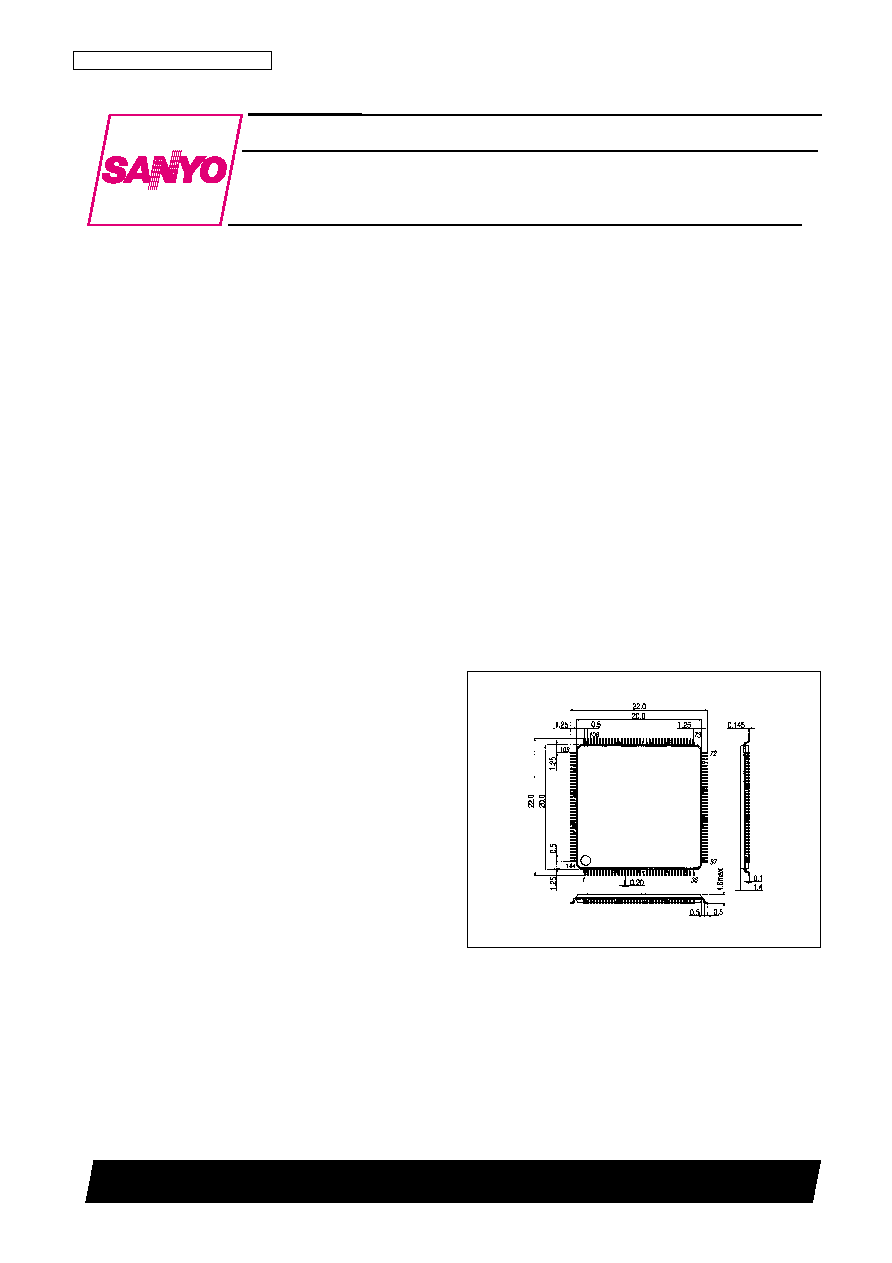
Package Dimensions
unit: mm
3214-SQFP144
CMOS IC
62698RM (OT) No. 5846-1/7
Preliminary
SANYO: SQFP144
[LC82221L]
SANYO Electric Co.,Ltd. Semiconductor Bussiness Headquarters
TOKYO OFFICE Tokyo Bldg., 1-10, 1 Chome, Ueno, Taito-ku, TOKYO, 110-8534 JAPAN
Motion JPEG Decoder
LC82221L
Ordering number : EN
*
5846
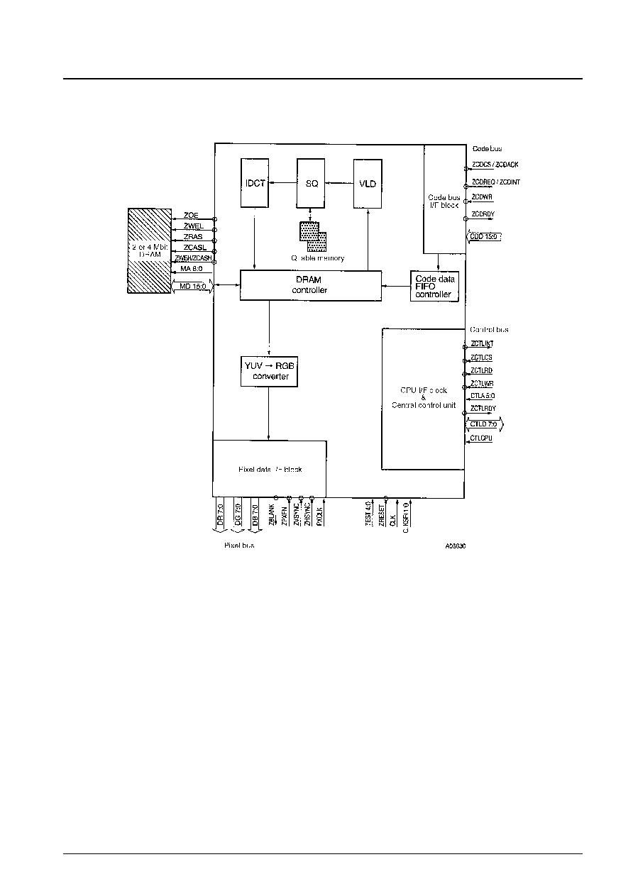
Block Diagram
No. 5846-2/7
LC82221L
No. 5846-3/7
LC82221L
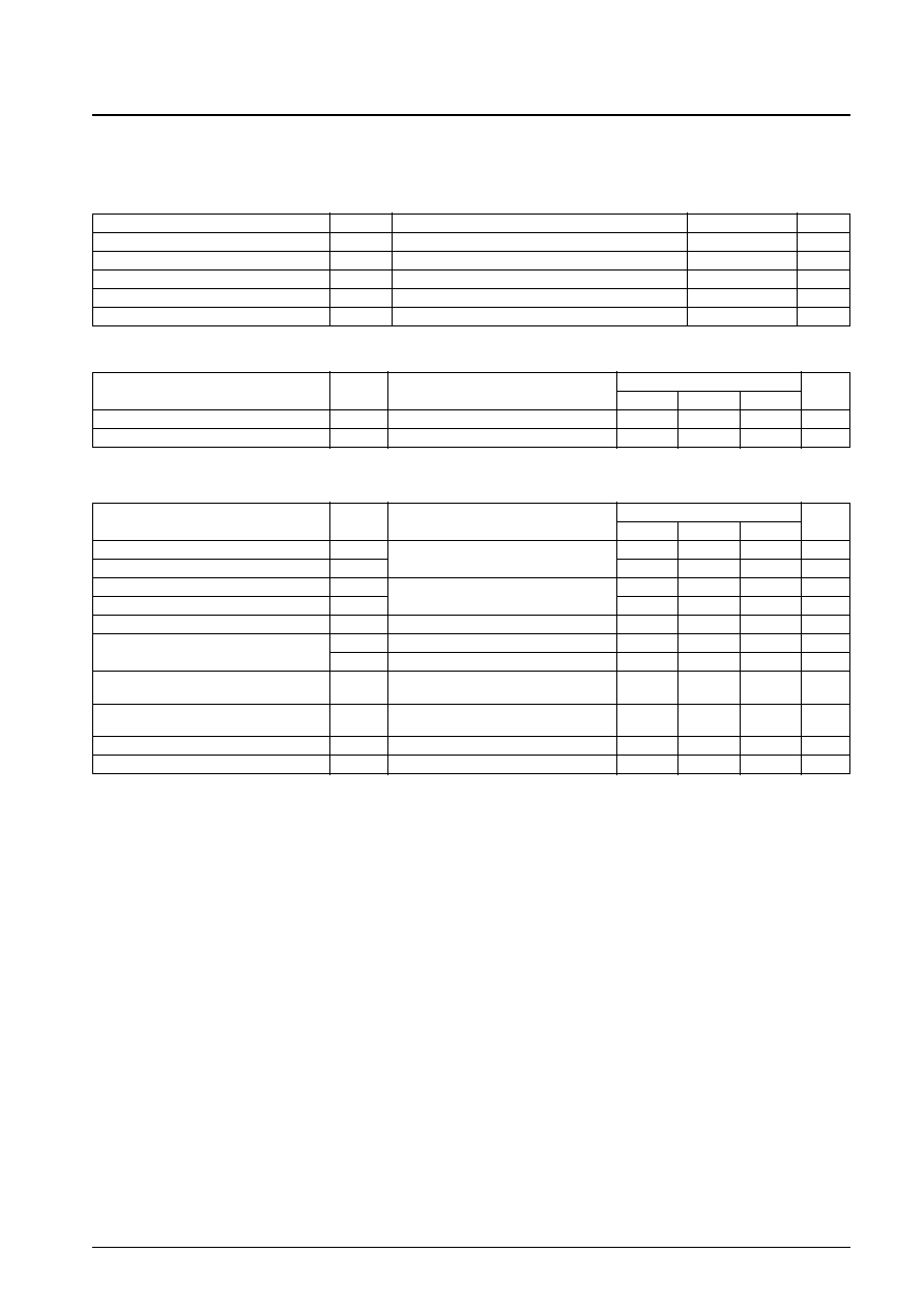
Parameter
Symbol
Conditions
Ratings
Unit
Maximum supply voltage
V
DD
≠0.3 to +4.6
V
Input and output voltage
V
I
, V
O
≠0.3 to V
DD
+0.3
V
Input and output current
I
I
, I
O
≠20 to +20
mA
Operating temperature
Topr
≠30 to +70
∞C
Storage temperature
Tstg
≠55 to +125
∞C
Absolute Maximum Ratings
at V
SS
= 0 V
Specifications
Electrical Characteristics
Parameter
Symbol
Conditions
Ratings
Unit
min
typ
max
Supply voltage
V
DD
3.0
3.3
3.6
V
Input voltage
V
IN
0
V
DD
V
Allowable Operating Ranges
at Ta = ≠30 to +70∞C
Parameter
Symbol
Conditions
Ratings
Unit
min
typ
max
Input high-level voltage
V
IH
1
CMOS level inputs: (1)
0.7 V
DD
V
Input low-level voltage
V
IL
1
0.2 V
DD
V
Input high-level voltage
V
IH
2
CMOS level Schmitt inputs: (2)
0.75 V
DD
V
Input low-level voltage
V
IL
2
0.15 V
DD
V
Input high-level current
I
IH
V
IN
= V
DD
; All input pins (including bus pins)
≠10
+10
µA
Input low-level current
I
IL
1
V
IN
= V
SS
: (3)
≠10
+10
µA
I
IL
2
V
IN
= V
DD
; Pins with pull-up resistors: (4)
≠100
≠10
µA
Output high-level voltage
V
OH
I
OH
= ≠6 mA; All output pins
V
DD
≠ 0.8
V
(including bus pins)
Output low-level voltage
V
OL
I
OL
= 6 mA; All output pins
0.4
V
(including bus pins)
Output leakage current
I
OZ
When set to high-impedance output: (5)
≠10
+10
µA
Pull-up resistance
R
UP
(6)
70
140
280
k
DC Characteristics
at Ta = ≠30 to +70∞C, V
DD
= 3.0 to 3.6 V, V
SS
= 0 V
Applicable Pins
(1) CTLCPU, CTLA, CTLD, CLKSEL, CLK, CDD, TEST, MD, DG, DB, DR, ZPXEN, ZHSYNC, ZVSYNC, PXCLK
(2) ZCTLCS, ZCTLRD, ZCTLWR, ZRESET, ZCDCS, ZCDWR
(3) CTLCPU, CTLA, CTLD, CLKSEL, CLK, CDD, TEST, DG, DB, DR, ZPXEN, ZHSYNC, ZVSYNC, PXCLK, ZCTLCS, ZCTLRD, ZCTLWR, ZRESET,
ZCDCS, ZCDWR
(4) MD
(5) ZCTLRDY, CTLD, ZCDRDY, MD, DG, DB, DR
(6) MD
No. 5846-4/7
LC82221L
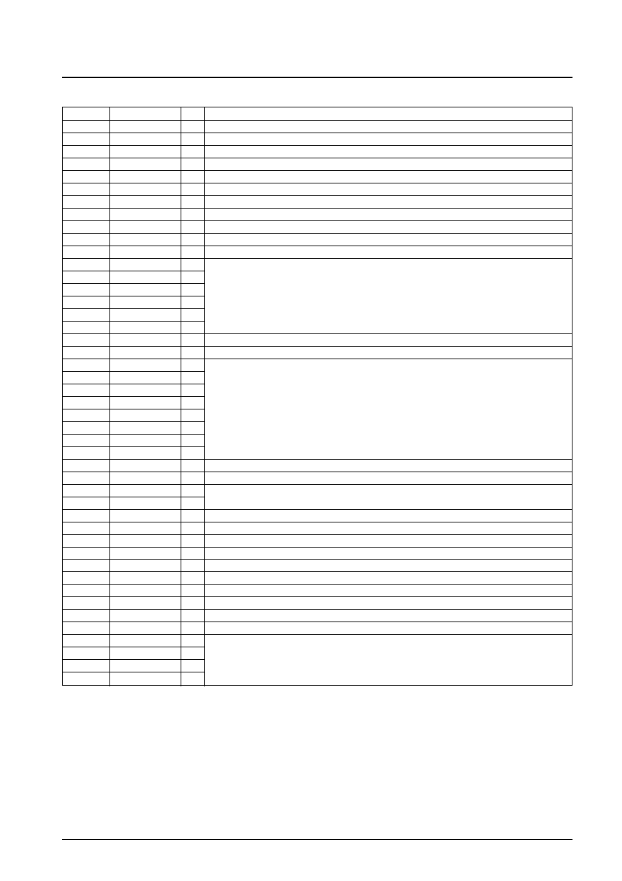
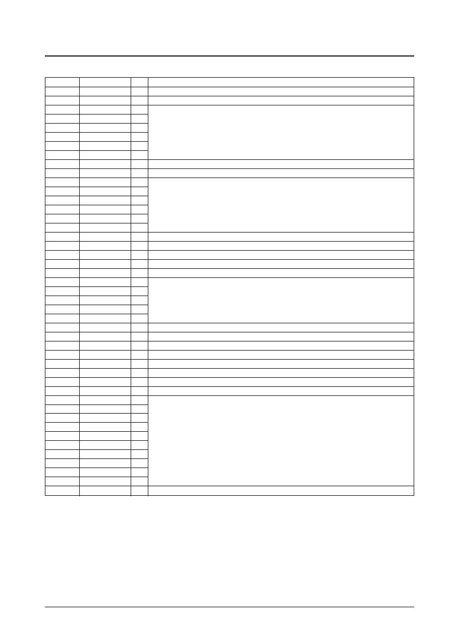
Pin Number
Pin Name
Type
Description
1
V
SS
Ground
2
ZCTLINT
O
Control bus interrupt request
3
ZCTLCS
I
Control bus select
4
ZCTLRD/RW
I
Control bus read or R/W select
5
ZCTLWR/DS
I
Control bus write/data strobe
6
ZCTLRDY
O
Control bus ready (tri-state output)
7
CTLCPU
I
Control bus CPU type selection
8
V
DD
+3.3-V power supply
9
V
SS
Ground
10
NC
11
NC
12
CTLA5
I
13
CTLA4
I
14
CTLA3
I
Control bus address
15
CTLA2
I
16
CTLA1
I
17
CTLA0
I
18
V
DD
+3.3-V power supply
19
V
SS
Ground
20
CTLD7
I/O
21
CTLD6
I/O
22
CTLD5
I/O
23
CTLD4
I/O
Control bus data
24
CTLD3
I/O
25
CTLD2
I/O
26
CTLD1
I/O
27
CTLD0
I/O
28
V
DD
+3.3-V power supply
29
V
SS
Ground
30
CLKSEL0
I
Clock divisor setting
31
CLKSEL1
I
CLKSEL1:0 = 00: No divisor, 01: Divisor = 2, 10: Divisor = 3.
32
CLK
I
System (decode) clock input
33
NC
34
ZRESET
I
Hardware reset
35
NC
36
V
SS
Ground
37
V
DD
+3.3-V power supply
38
ZCDCS/ZCDACK
I
Code bus select/code bus DMA acknowledge
39
ZCDINT/ZCDREQ
O
Code bus interrupt/code bus DMA request
40
ZCDWR
I
Code bus data write signal
41
ZCDRDY
O
Code bus ready (tri-state output)
42
CDD15
I
43
CDD14
I
Code bus data
44
CDD13
I
(CDD8 to CDD15 are unused in 8-bit mode.
*
)
45
CDD12
I
Pin Functions
Continued on next page.
Note:
*
These pins must be pulled up with a resistance of about 10 k
.
No. 5846-5/7
LC82221L
Continued from preceding page.
Pin Number
Pin Name
Type
Description
46
V
DD
+3.3-V power supply
47
V
SS
Ground
48
CDD11
I
49
CDD10
I
50
CDD9
I
Code bus data
51
CDD8
I
52
CDD7
I
53
CDD6
I
54
V
DD
+3.3-V power supply
55
V
SS
Ground
56
CDD5
I
57
CDD4
I
58
CDD3
I
Code bus data
59
CDD2
I
60
CDD1
I
61
CDD0
I
62
V
SS
+3.3-V power supply
63
V
DD
Ground
64
NC
65
NC
66
NC
67
TEST0
I
68
TEST1
I
69
TEST2
I
Test pins
*
70
TEST3
I
71
TEST4
I
72
V
SS
Ground
73
V
DD
+3.3-V power supply
74
ZOE
O
Memory output enable
75
ZWEL
O
Memory write enable (L)
76
ZRAS
O
Row address strobe
77
ZCASL
O
Column address strobe (L)
78
ZWEH/ZCASH
O
Memory write enable (H)/column address strobe (H)
79
V
SS
Ground
80
MD15
I/O
81
MD14
I/O
82
MD13
I/O
83
MD12
I/O
84
MD11
I/O
Frame memory interface data bus
85
MD10
I/O
86
MD9
I/O
87
MD8
I/O
88
MD7
I/O
89
MD6
I/O
90
V
DD
+3.3-V power supply
Continued on next page.
Note:
*
These pins must be tied to ground.