 | –≠–ª–µ–∫—Ç—Ä–æ–Ω–Ω—ã–π –∫–æ–º–ø–æ–Ω–µ–Ω—Ç: LC83025E | –°–∫–∞—á–∞—Ç—å:  PDF PDF  ZIP ZIP |
CMOS LSI
Ordering number : EN4977A
62896HA (OT)/63095HA (OT) No. 4977-1/15
SANYO Electric Co.,Ltd. Semiconductor Bussiness Headquarters
TOKYO OFFICE Tokyo Bldg., 1-10, 1 Chome, Ueno, Taito-ku, TOKYO, 110 JAPAN
Digital Signal Processor
for Karaoke Products
LC83025E
Overview
The LC83025E is a special-purpose karaoke DSP that
implements the signal processing required by karaoke
systems, including pitch shift, microphone echo, voice
muting and simple surround, with only a single 256Kb
external DRAM. Since the LC83025E includes built-in
A/D and D/A converters, it can also handle analog inputs
and outputs in addition to digital inputs and outputs. The
LC83025E uses serial transfer of coefficient data from a
microcontroller to handle changes in functions and
characteristics required for each application.
Features
∑ Applications
-- Pitch shift
The LC83025E can shift the music pitch or the
microphone pitch by ±15 steps in 1/4 interval steps,
or ±1 octave in scale tone steps according to
command data sent from the microcontroller.
Furthermore, the pitch can be changed up to ±1
octave in arbitrary steps by setting internal
coefficients.
-- Microphone echo
The LC83025E implements echo processing for the
signal input from the microphone A/D converter.
The amount of echo, the delay time and other
parameters can be changed by setting coefficients.
-- Voice mute
The LC83025E implements processing that removes
monaural signal components included in the music
signal. This allows CDs with vocals to be used as
karaoke CDs. Command data is used to turn the
voice mute function on or off.
-- Simple surround
The LC83025E implements a simple surround
function by adding delayed components to the music
signal. The LC83025E includes six sets of simple
surround coefficients as built-in preset data. These
values can be switched by sending command data.
Applications can implement their own original
surround effects by setting the coefficients.
However, the algorithm itself is fixed.
-- Flexible input mixing
The LC83025E supports hybrid mixing of digital
and analog left and right channel song inputs, and
thus can handle a wide range of disk processing
configurations.
∑ Audio inputs and outputs
-- Inputs: Digital - One system (stereo)
A/D converter - Three channels
-- Outputs: Digital - One system (stereo)
D/A converter - Two channels
-- A/D converter
Second order
modulation - Three channels
-- D/A converter
4
◊
oversampling digital filters
plus second order noise shaper
plus 5-bit PWM system - Two channels
∑ Master clock: 768 fs
∑ External memory: Up to two 256K (64K
◊
4-bit)
DRAMs can be used
∑ Microcontroller input: Synchronous 8-bit serial data
∑ Supply voltage: 5 V single-voltage
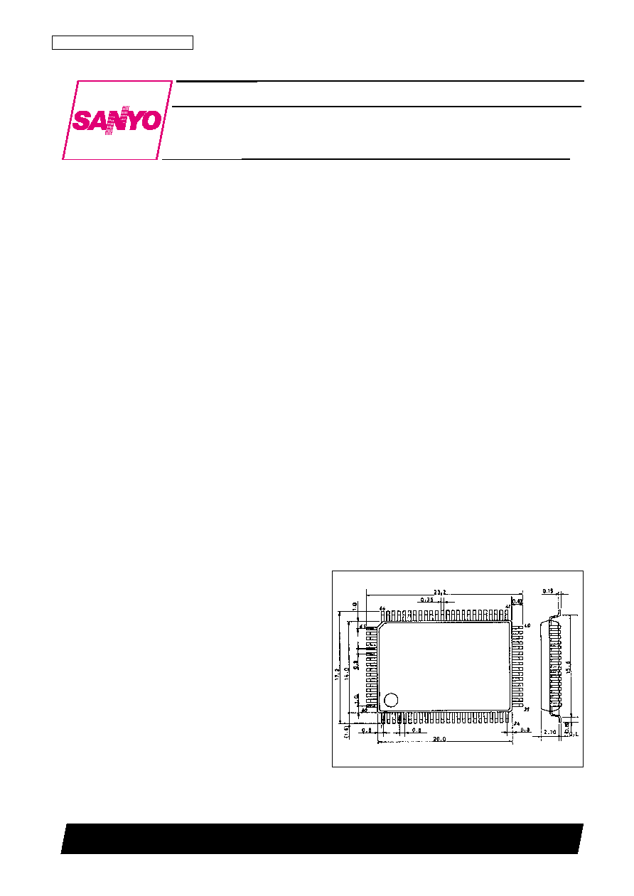
∑ Package: QFP80E
Package Dimensions
unit: mm
3174-QFP80E
SANYO: QFP80E
[LC83025E]
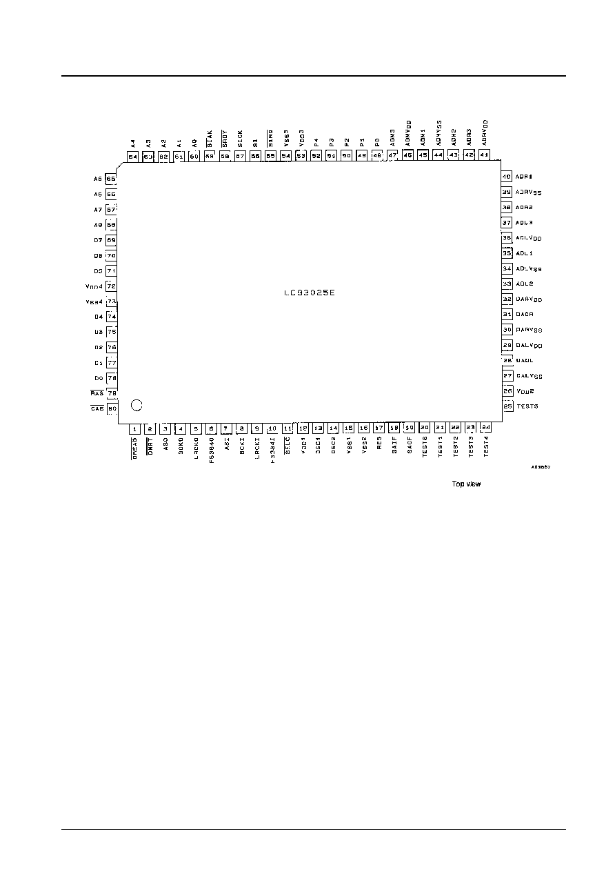
Pin Assignment
No. 4977-2/15
LC83025E
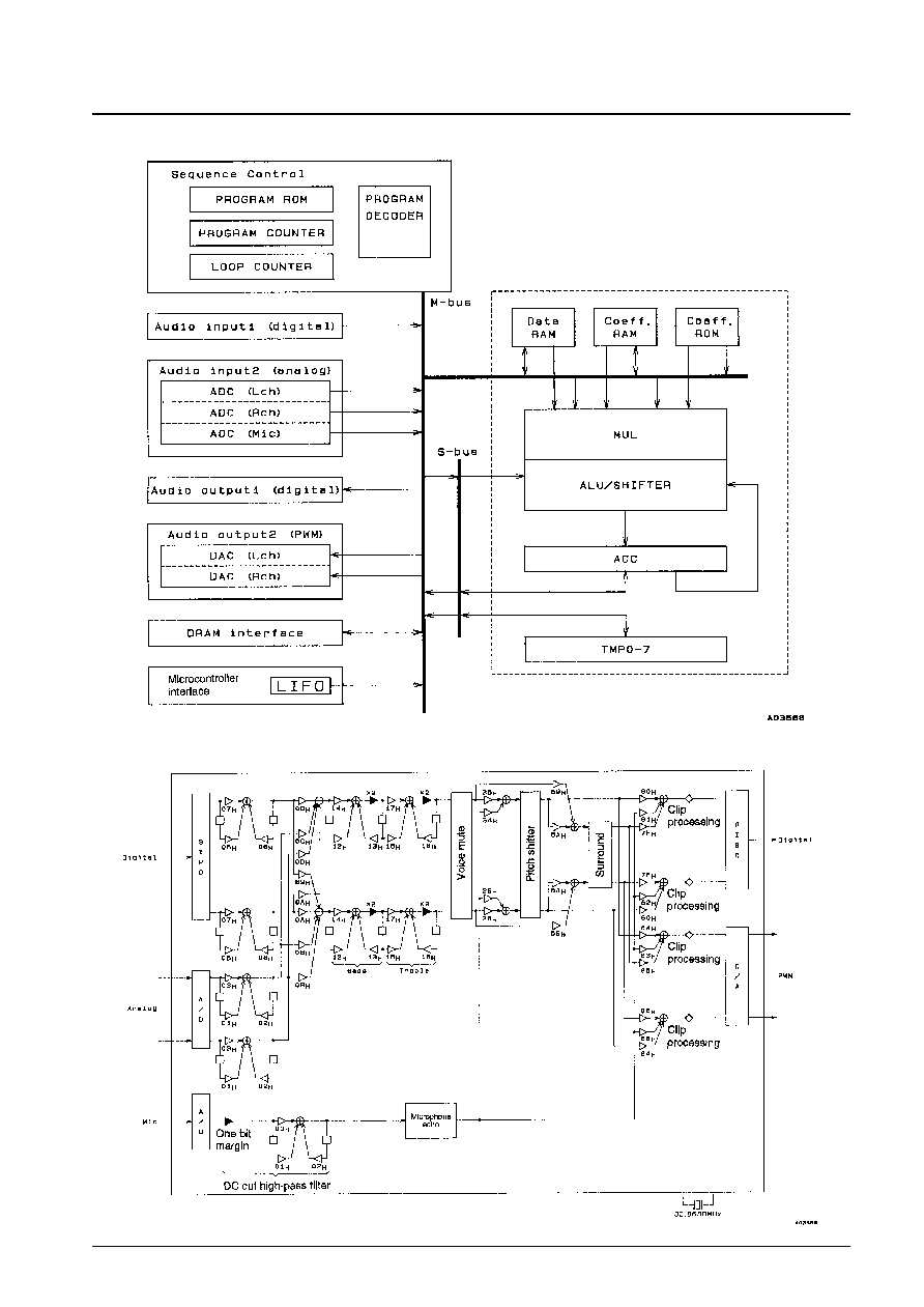
Block Diagram
Signal Flow Overview
No. 4977-3/15
LC83025E
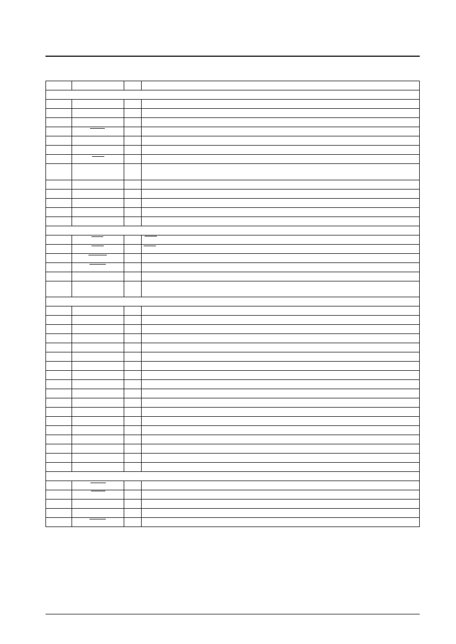
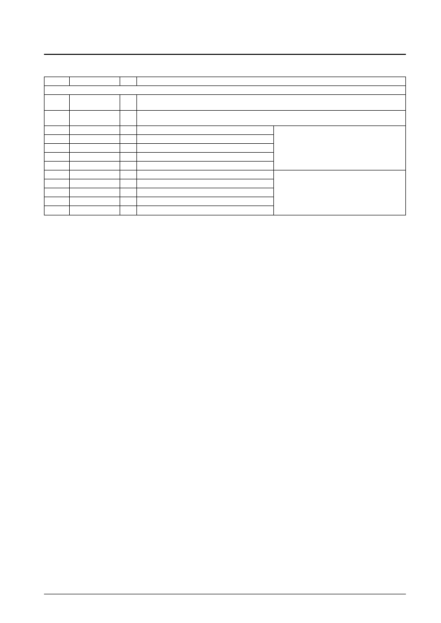
Pin Functions
No. 4977-4/15
LC83025E
Pin No.
Symbol
I/O
Function
[Control pins]
13
OSC1
I
Crystal oscillator connection (768 fs)
14
OSC2
O
Crystal oscillator connection (768 fs)
10
FS384I
I
384 fs input (Apply a clock that is equal to the OSC1/OSC2 768 fs clock divided by 2.)
11
SELC
I
Audio clock source switching (High: Fixes FS384I as the clock)
18
SAIF
I
Digital audio input mode switching (Low: backward packed, High: forward packed)
19
SAOF
I
Digital audio output mode switching (Low: 48 fs, High: 64 fs)
17
RES
I
Reset
25 to 21
TEST5 to
I
Test (Must be tied to ground in normal operation.)
TEST1
20
TEST6
O
Test (Must be left open in normal operation.)
48
P0
I
Coefficient transfer mode switching
50, 49
P2, P1
I
Initial operating mode setting (This pin should be held high in normal operation.)
51
P3
O
Microphone signal present (low output) or absent (high output) indication output
52
P4
O
Music signal present (low output) or absent (high output) indication output
[External memory interface]
79
RAS
O
RAS signal output
80
CAS
O
CAS signal output
1
DREAD
O
External memory read signal output
2
DWRT
O
External memory write signal output
68 to 60
A8 to A0
O
Address outputs
69 to 71,
D7 to D0
I/O
Data I/O (Normally, only D3 to D0 are used.)
74 to 78
[Audio interface]
9
LRCKI
I
ASI L/R clock input (1 fs)
5
LRCKO
O
ASO L/R clock output (1 fs)
8
BCKI
I
ASI bit clock input (32 fs or higher)
4
BCKO
O
ASO bit clock output (48 fs or 64 fs)
6
FS384O
O
ASO 384 fs output
7
ASI
I
Digital audio data input (MSB first, 16 bits)
3
ASO
O
Digital audio data output (MSB first, backward packed, 16 bits)
35
ADL1
I
A/D converter input (left channel)
33
ADL2
O
A/D converter output (left channel)
37
ADL3
O
A/D converter output (left channel)
40
ADR1
I
A/D converter input (right channel)
38
ADR2
O
A/D converter output (right channel)
42
ADR3
O
A/D converter output (right channel)
45
ADM1
I
A/D converter input (microphone)
43
ADM2
O
A/D converter output (microphone)
47
ADM3
O
A/D converter output (microphone)
28
DAOL
O
D/A converter output (left channel)
31
DAOR
O
D/A converter output (right channel)
[Microcontroller interface]
55
SIRQ
I
Serial input request signal input
59
SIAK
O
Output indicating serial input execution in progress
56
SI
I
Serial data input from the control microcontroller (8-bit serial data)
57
SICK
I
SI transfer clock input
58
SRDY
I
Ready signal input from the control microcontroller that indicates that serial data input has completed
Continued on next page.
Continued from preceding page.
No. 4977-5/15
LC83025E
Pin No.
Symbol
I/O
Function
[Power supply pins]
12, 26,
V
DD
--
V
DD
for the digital block (Connect to +5 V.)
53, 72
(Keep connections as short as possible so that potential differences between the V
DD
pins do not occur.)
15, 16,
V
SS
--
V
SS
for the digital block (Connect to ground.)
54, 73
(Keep connections as short as possible so that potential differences between the V
SS
pins do not occur.)
36
ADLV
DD
--
A/D converter V
DD
(left channel) (Connect to +5 V.)
41
ADRV
DD
--
A/D converter V
DD
(right channel) (Connect to +5 V.)
46
ADMV
DD
--
A/D converter V
DD
(microphone) (Connect to +5 V.)
29
DALV
DD
--
D/A converter V
DD
(left channel) (Connect to +5 V.)
32
DARV
DD
--
D/A converter V
DD
(right channel) (Connect to +5 V.)
34
ADLV
SS
--
A/D converter V
SS
(left channel) (Connect to ground.)
39
ADRV
SS
--
A/D converter V
SS
(right channel) (Connect to ground.)
44
ADMV
SS
--
A/D converter V
SS
(microphone) (Connect to ground.)
27
DALV
SS
--
D/A converter V
SS
(left channel) (Connect to ground.)
30
DARV
SS
--
D/A converter V
SS
(right channel) (Connect to ground.)
Design the application wiring so
that potential differences do not
occur between the analog V
SS
pins and between the digital V
SS
group and the analog V
SS
group.
Design the application wiring so
that potential differences do not
occur between the analog V
DD
pins and between the digital V
DD
group and the analog V
DD
group.