 | –≠–ª–µ–∫—Ç—Ä–æ–Ω–Ω—ã–π –∫–æ–º–ø–æ–Ω–µ–Ω—Ç: LC83026E | –°–∫–∞—á–∞—Ç—å:  PDF PDF  ZIP ZIP |

Overview
The LC83026E provides the audio signal processing
required in karaoke systems, including pitch shift,
microphone echo, voice muting, and simple surround
simulation. It is a special-purpose DSP that implements
karaoke processing with the addition of a single external
256-Kb DRAM. The LC83026E includes on-chip A/D and
D/A converters and supports both digital and analog
inputs and outputs. Its functions and characteristics can be
modified to match the needs of the end product by sending
coefficient data from the microcontroller over a serial
interface.
Features
∑ Application features
-- Pitch shift
The LC83026E supports pitch shifting of ±15
quarter tone steps, or ±1 octave in scale tone units as
specified by command data. This pitch shifting can
be applied either to the music track or to the
microphone input. It is also possible to set up pitch
shifting of ±1 octave in arbitrary steps by setting
coefficient values.
-- Microphone echo
The LC83026E can apply echo processing to the
input signal from the microphone A/D converter.
The echo coefficients, including amount of echo and
delay time, can be set.
-- Voice muting
The LC83026E provides attenuation of monaural
components in the music signal. This allows CDs
that include vocals to be used for karaoke. The voice
muting function is turned on or off by command data
transferred over the serial interface.
-- Simple surround
The LC83026E implements a simple surround
simulation function by adding delay components to
the music signal. The LC83026E includes six sets of
simple surround coefficients as preset data, and these
can be selected and switched using command data
transferred over the serial interface. User-original
surround effects can be implemented by setting
coefficients, but the algorithm is fixed.
-- Versatile input mixing
The LC83026E supports hybrid mixing of digital
music inputs and analog music inputs for both the
left and right channels to support the processing of a
wide range of disks.
∑ Audio inputs and outputs
-- Inputs: Digital
One system (stereo)
A/D converters
Three channels
-- Outputs: Digital
One system (stereo)
D/A converters
Two channels
-- A/D converters
Second-order delta-sigma modulation
Three channels
-- D/A converters
2
◊
oversampling digital filters + third-order noise
shaper system
Two channels
∑ Master clock: 768fs
∑ External memory: Up to two 256K (64K
◊
4 bits)
external DRAMs can be used.
∑ Microcontroller input: Synchronous 8-bit serial data
∑ Power-supply voltage: 5V single-voltage supply
∑ Package: QFP80E
Package Dimensions
unit: mm
3174-QFP80E
CMOS IC
Ordering number : EN5663
63097HA(OT) No. 5663-1/16
SANYO: QIP80E
[LC83026E]
SANYO Electric Co.,Ltd. Semiconductor Bussiness Headquarters
TOKYO OFFICE Tokyo Bldg., 1-10, 1 Chome, Ueno, Taito-ku, TOKYO, 110 JAPAN
Digital Signal Processor for Karaoke Systems
LC83026E
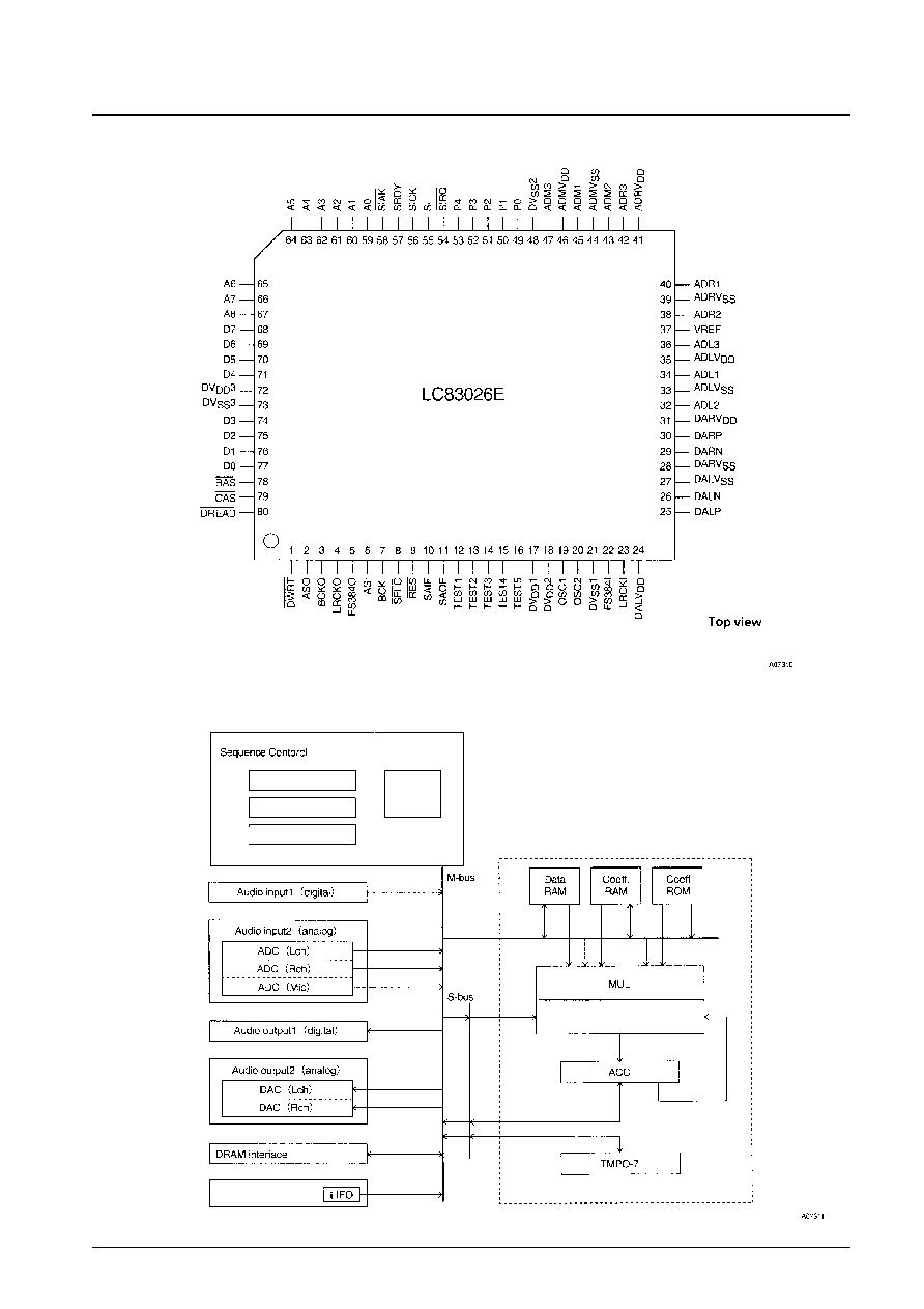
Pin Assignment
Block Diagram
No. 5663-2/16
LC83026E
Microcontroller
interface
Program
decoder
Program ROM
Program counter
Loop counter
No. 5663-3/16
LC83026E
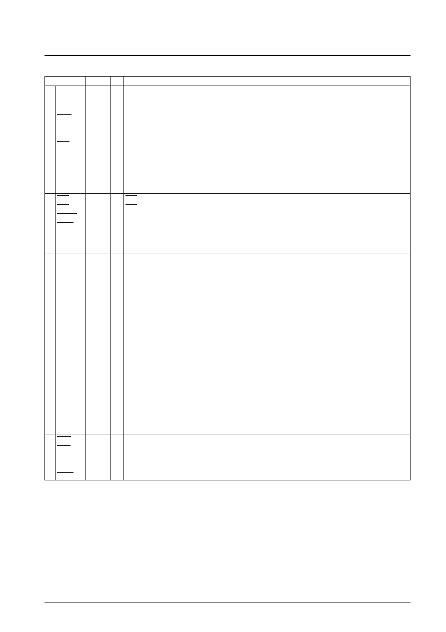
Pin Functions
Pin
Pin No.
I/O
Function
OSC1
19
I
Crystal oscillator connection (768fs)
OSC2
20
O
Crystal oscillator connection (768fs)
FS384I
22
I
384fs input
SELC
8
I
Audio clock source switching (High: external, low: internal)
SAIF
10
I
Digital audio input mode switching (Low: backward packing, high: forward packing)
SAOF
11
I
Digital audio output mode switching (Low: 48fs, high 64fs)
RES
9
I
Reset
TEST5 to 1 16 to 12
I
Test (Must be connected to ground during normal operation.)
P0
49
I
Coefficient transfer mode control
P2 to P1
51, 50
I
Initial operating mode control (A high level should be applied for normal operation.)
P3
52
O
Microphone signal input level: Yes (low output)/No (high output) output
P4
53
O
Music signal input level: Yes (low output)/No (high output) output
RAS
78
O
RAS signal output
CAS
79
O
CAS signal output
DREAD
80
O
External memory read signal output
DWRT
1
O
External memory write signal output
A8 to A0
67 to 59
O
Address output
D7 to D0
68 to 71,
I/O
Data input and output (Normally only D0 to D3 are used)
74 to 77
LRCKI
23
I
ASI L/R clock input (1fs)
LRCKO
4
O
ASO L/R clock output (1fs)
BCKI
7
I
ASI bit clock input (32fs or higher)
BCKO
3
O
ASO bit clock output (48fs or 64fs)
FS384O
5
O
ASO 384fs output
ASI
6
I
Digital audio data input (16-bits, MSB first)
ASO
2
O
Digital audio data output (16-bits, MSB first, backward packed)
ADL1
34
I
A/D converter input (left channel)
ADL2
32
O
A/D converter output (left channel)
ADL3
36
O
A/D converter output (left channel)
ADR1
40
I
A/D converter input (right channel)
ADR2
38
O
A/D converter output (right channel)
ADR3
42
O
A/D converter output (right channel)
ADM1
45
I
A/D converter input (microphone)
ADM2
43
O
A/D converter output (microphone)
ADM3
47
O
A/D converter output (microphone)
DALP
25
O
D/A converter output (left channel)
DALN
26
O
D/A converter output (left channel)
DARP
30
O
D/A converter output (right channel)
DARN
29
O
D/A converter output (right channel)
SIRQ
54
I
Input for the serial input request signal
SIAK
58
O
Output that indicates that a serial input is in progress
SI
55
I
Serial data input from the control microcontroller (8-bit serial input)
SICK
56
I
SI pin transfer clock input
SRDY
57
I
Ready signal input (from the control microcontroller) that indicates the completion of a serial data input.
Control pins
External memory interface
Audio interface
Microcontroller interface
Continued on next page.
No. 5663-4/16
LC83026E
Continued from preceding page.
Pin
Pin No.
I/O
Function
DV
DD
1 to 3 17, 18, 72
--
Digital block V
DD
(Must be connected to +5 V.)
<Make connections as short as possible so that no potential differences occur between any of the V
DD
pins.>
DV
SS
1 to 3 21, 48, 73
--
Digital block V
SS
(Must be connected to ground.)
<Make connections as short as possible so that no potential differences occur between any of the V
SS
pins.>
ADLV
DD
35
--
A/D converter V
DD
(left channel) (Connect to +5 V.)
ADRV
DD
41
--
A/D converter V
DD
(right channel) (Connect to +5 V.)
ADMV
DD
46
--
A/D converter V
DD
(microphone) (Connect to +5 V.)
DALV
DD
24
--
D/A converter V
DD
(left channel) (Connect to +5 V.)
DARV
DD
31
--
D/A converter V
DD
(right channel) (Connect to +5 V.)
ADLV
SS
33
--
A/D converter V
SS
(left channel) (Connect to ground.)
ADRV
SS
39
--
A/D converter V
SS
(right channel) (Connect to ground.)
ADMV
SS
44
--
A/D converter V
SS
(microphone) (Connect to ground.)
DALV
SS
27
--
D/A converter V
SS
(left channel) (Connect to ground.)
DARV
SS
28
--
D/A converter V
SS
(right channel) (Connect to ground.)
Power supply
Design the wiring so that potential differences do
not occur between the analog system V
DD
pins and
either other analog system V
DD
pins or the digital
system V
DD
pins.
Design the wiring so that potential differences do
not occur between the analog system V
SS
pins and
either other analog system V
SS
pins or the digital
system V
SS
pins.
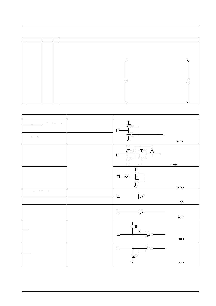
Pin Circuits
Pins
Specifications
Circuit
ASO, LRCKO, BCKO, RAS, CAS,
DREAD, DWRT, FS384O, A0 to A8
TTL output
ADL2, ADL3, ADM2, ADM3, ADR2,
ADR3
Analog output
Schmitt input
DALP, DALN, DARP, DARN
SI, SICK, SIRQ, SRDY, (OSC1)
Low Schmitt input
FS384I, BCKI, ASI, LRCKI
Normal input
TEST1 to TEST5
Input with built-in pull-up resistor
RES
Input with built-in pull-down resistor
SELC, SAIF, SAOF
P3, P4, SIAK
CMOS intermediate current output
Continued on next page.
Output data
Output data
Output data
Input data
Input data
Input data
Input data
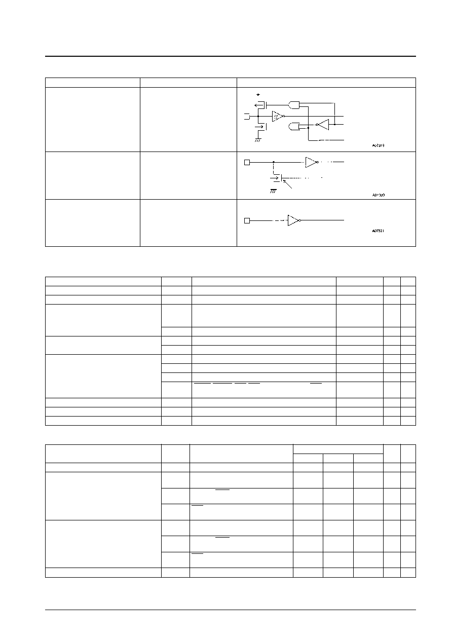
No. 5663-5/16
LC83026E
Continued from preceding page.
Pins
Specifications
Circuit
D0 to D7
CMOS intermediate current output
Low Schmitt input
P0 to P2
N-channel open drain intermediate
current output
Normal input
ADL1, ADR1, ADM1
Analog input
Parameter
Symbol
Conditions
Ratings
Unit
Notes
Maximum supply voltage
V
DD
max
≠0.3 to +7.0
V
Input voltage
V
IN
≠0.3 to V
DD
+0.3
V
Values up to the
V
O
1
OSC2 output
oscillator voltage are
V
Output voltage
allowable.
V
O
2
Outputs other than OSC2
≠0.3 to V
DD
+0.3
V
Peak output current
I
OP
1
Audio interface, external RAM interface
≠2 to +4
mA
1
I
OP
2
Microcontroller interface, P3, P4
≠2 to +10
mA
2
I
OA
1
Audio interface, external RAM interface: Per pin
≠2 to +4
mA
1
I
OA
2
Microcontroller interface, P3, P4: Per pin
≠2 to +10
mA
2
Average output current
I
OA
1
FS384O, LRCKO, BCKO, ASO : Total
≠10 to +10
mA
I
OA
2
DWRT, DREAD, RAS, CAS, A0 to A8, D0 to D7, SIAK,
≠10 to +10
mA
P3, P4 : Total
Allowable power dissipation
Pd max
Ta = ≠30 to +70∞C
700
mW
Operating temperature
Topr
≠30 to +70
∞C
Storage temperature
Tstg
≠40 to +125
∞C
Specifications
Absolute Maximum Ratings
at Ta = 25∞C, V
SS
= 0 V
Parameter
Symbol
Conditions
Ratings
Unit Notes
min
typ
max
Operating supply voltage
V
DD
4.75
5.25
V
V
IH
1
Audio interface and external RAM
2.4
V
4
interface
Input high-level voltage
V
IH
2
P0 to P2, SELC, SAIF, SAOF,
0.7 V
DD
V
5
TEST1 to TEST5
V
IH
3
RES, OSC1, and the microcontroller
0.75 V
DD
V
6
interface
V
IL
1
Audio interface and external RAM
0.8
V
4
interface
Input low-level voltage
V
IL
2
P0 to P2, SELC, SAIF, SAOF,
0.3 V
DD
V
5
TEST1 to TEST5
V
IL
3
RES, OSC1, and the microcontroller
0.25 V
DD
V
6
interface
Instruction cycle time
t
CYC
58
59.11
ns
Allowable Operating Ranges
at Ta = ≠30 to +70∞C, all V
DD
= 4.75 to 5.25 V, all V
SS
= 0 V unless otherwise specified
Continued on next page.
Input data
Input data
Input data
Test output data
Off during normal operation
I/O control
Output data