Ordering number : ENN
*
6327
21800RM (OT) No. 6237-1/7
Overview
The LC85050 is a cordless answering machine system IC
that integrates an extensive set of functions on a single
chip. These functions include a DSP that provides audio
recording and playback functions, voice recognition
functions, text-to-speech synthesis, and line and audio
echo cancellation, a
A/D converter, a
D/A
converter, a flash memory interface, and a host CPU
interface.
The LC85050 uses the PULCOD
TM
(pulse code excited
linear prediction) high-compression ratio compression
algorithm to allow up to 19 minutes of audio recording on
4M of external flash memory. Furthermore, the optional
LD-ADPCM (low-distortion ADPCM) waveform
encoding algorithm allows the recording and playback of
high-quality audio signals.
The LC85050's line and audio echo cancellation function
allows it to implement a speakerphone function for
answering machine/telephone products. It also includes
ITU-T V.23 and Bell 202 conforming data transmission
and reception functions to support caller ID.
The LC85050's text-to-speech synthesis function allows
end products to announce the name of the calling party. Its
speaker-independent voice recognition function can be
used to allow users to easily enter telephone numbers in its
phone book. The LC85050's speaker-dependent voice
recognition function allows users to pre-register the names
of people to call with the user's own voice. Then the user
can then either recall any of those parties' phone number,
or even call the person, simply by speaking the name.
Furthermore, the LC85050 can easily implement all of the
functions required by standard telephone or answering
machine products, including DTMF and other tone
generation and detection as well as music synthesis.
Features
� PULCOD
TM
(high compression ratio encoding)
--High compression ratio: 3.6 kbps
--Automatic input gain adjustment function
--Voice trigger function
--Silence removal function
--Tail cut function
--Variable-speed playback function
Preliminary
LC85050
SANYO Electric Co.,Ltd. Semiconductor Company
TOKYO OFFICE Tokyo Bldg., 1-10, 1 Chome, Ueno, Taito-ku, TOKYO, 110-8534 JAPAN
Cordless Answering Machine System IC
CMOS IC
Any and all SANYO products described or contained herein do not have specifications that can handle
applications that require extremely high levels of reliability, such as life-support systems, aircraft's
control systems, or other applications whose failure can be reasonably expected to result in serious
physical and/or material damage. Consult with your SANYO representative nearest you before using
any SANYO products described or contained herein in such applications.
SANYO assumes no responsibility for equipment failures that result from using products at values that
exceed, even momentarily, rated values (such as maximum ratings, operating condition ranges, or other
parameters) listed in products specifications of any and all SANYO products described or contained
herein.
Continued on next page.
0.15
1.6
14.0
17.2
0.8
1
24
25
40
41
64
65
80
21.6
0.8
3.0max
1.0
2.7
15.6
0.8
1.6
0.35
23.2
20.0
0.8
0.8
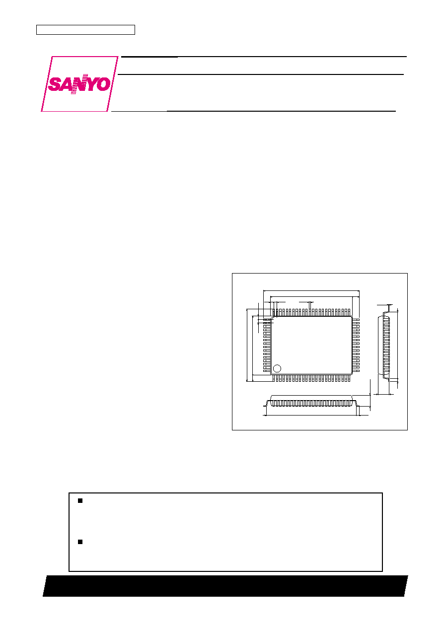
SANYO: QFP80E (QIP80E)
[LC85050]
Package Dimensions
unit: mm
3174-QIP80E
� LD-ADPCM function (waveform encoding) (optional
function)
--Compression ratio: 14.4, 21.6, and 28.8 kbps
--Automatic input gain adjustment function
--Voice trigger function
--Tail cut function
� Text-to-speech synthesis function
--Accent adjustment
--Katakana input
� Voice recognition function
--Speaker-independent recognition (15 words)
--Speaker-dependent recognition (50 words)
� Flash memory management function (8M address space)
--Flash memory: 4 M (
�
1 or
�
8)
� Full-duplex hands-free function
--Line echo canceler
--Audio echo canceler for speakerphone operation
--Telephone conversation recording using LD-ADPCM (option)
--DTMF detection
--Caller ID detection
� Modem functions
--Bell 202 (1200 bps) send/receive
--ITU-T V.23 (1200 bps) send/receive
--Synchronous/asynchronous communication functions
Start/stop synchronization, HDLC, DDI, and NTT
support
--Programmable reception sensitivity
(�10 dBm to �47 dBm)
� Programmable tone generation and detection
--Individually adjustable reception sensitivity
(�10 dBm to �47 dBm)
� DTMF generation and detection
� Call progress tone detection
--Adjustable reception sensitivity
(�10 dBm to �47 dBm)
� Melody function (option)
� Programmable transmission level (0 dBm to �15 dBm)
� Reception dynamic range: 0 to �47 dBm
� Self-diagnostic function
� Monitor output function
� Host CPU interface
--3-wire serial interface (clock synchronous)
--8-bit parallel interface
� Output ports (up to 12 ports):
3 output ports are always available.
� Low-power CMOS
� Supply voltage
--Single 3.3 V supply, or dual 3.3 and 5.0 V supply
voltages
� Package: QIP-80E
No. 6237-2/7
LC85050
Continued from preceding page.
Parameter
Symbol
Conditions
Ratings
Unit
Maximum supply voltage
V
DD
3
�0.3 to +4.2
V
V
DD
5
�0.3 to +6.0
V
I/O voltages
V
I
3, V
O
3
�0.3 to V
DD
3 + 0.3
V
V
I
5, V
O
5
�0.3 to V
DD
5 + 0.3
V
Allowable power dissipation
Pdmax
Ta
25�C
500
mW
Operating temperature
Topr
�30 to +70
�C
Storage temperature
Tstg
�55 to +125
�C
Soldering conditions
Hand soldering
3 seconds
350
�C
Reflow soldering
10 seconds
235
�C
Specifications
Absolute Maximum Ratings
at Ta = 25�C, GND = 0 V
Parameter
Symbol
Conditions
Ratings
Unit
min
typ
max
Supply voltage
V
DD
3
3.0
3.3
3.6
V
V
DD
5
3.0
5.0
5.5
V
Input voltage range
V
IN
3
0
V
DD
3
V
V
IN
5
0
V
DD
5
V
Allowable Operating Ranges
at Ta = �30 to +70�C, GND = 0 V
Applicable pins
V
I
3, V
O
3, V
IN
3: PLLI, PLLO, RIN, AUXO, AUXI, SPOUT, MIC, VREF, TXA, RXA
V
I
5, V
O
5, V
IN
5: All pins other than the above.
No. 6237-3/7
LC85050
Parameter
Symbol
Conditions
Ratings
Unit
min
typ
max
Input high-level voltage
V
IH
1
CMOS (1), (4)
0.7 V
DD
5
V
V
IH
2
CMOS Schmitt inputs (2)
0.8 V
DD
5
V
Input low-level voltage
V
IL
1
CMOS (1), (4)
0.3 V
DD
5
V
V
IL
2
CMOS Schmitt inputs (2)
0.2 V
DD
5
V
Output high-level voltage
V
OH
I
OH
= �4 mA (3), (4)
V
DD
5 � 2.1
V
Output low-level voltage
V
OL
I
OL
= 4 mA (3), (4)
0.4
V
Input leakage current
I
IL
V
I
= GND, V
DD
5
�10
+10
�A
Output leakage current
I
OZ
In the high-impedance output state
�10
+10
�A
Oscillator frequency
f
CLK
3.6864
MHz
Current drain
I
DD
1
Operating
110
150
mA
I
DD
1
In power down mode
5
�A
DC Characteristics (1)
at Ta = �30 to +70�C, GND = 0 V, V
DD
5 = 4.5 to 5.5 V, V
DD
3 = 3.0 to 3.6 V
The applicable pins are as follows.
(1) TESTER, TESTEN, TESTD, PS, XIN, RB1, RB0
(2) RESET, CPUCS, CPUOE, CPUWE
(3) BUSY, IREQ, PLOCK, PA0 to PA2, MCS0, MCS1, MWE, MRE, CLE, ALE, WP0, WP1, EYECLK, EYESYNC, EYED, XOUT
(4) CD0 to CD7, MD0 to MD7
Note: The PLLI, PLLO, RIN, AUXO, AUXI, SPOUT, MIC, VREF, RXA, and TXA pins are not included in the DC characteristics ratings.
Parameter
Symbol
Conditions
Ratings
Unit
min
typ
max
Input high-level voltage
V
IH
1
CMOS (1), (4)
0.7 V
DD
5
V
V
IH
2
CMOS Schmitt inputs (2)
0.75 V
DD
5
V
Input low-level voltage
V
IL
1
CMOS (1), (4)
0.2 V
DD
5
V
V
IL
2
CMOS Schmitt inputs (2)
0.15 V
DD
5
V
Output high-level voltage
V
OH
I
OH
= �2 mA (3), (4)
V
DD
5 � 0.8
V
Output low-level voltage
V
OL
I
OL
= 2 mA (3), (4)
0.4
V
Input leakage current
I
IL
V
I
= GND, V
DD
5
�10
+10
�A
Output leakage current
I
OZ
In the high-impedance output state
�10
+10
�A
Oscillator frequency
f
CLK
3.6864
MHz
Current drain
I
DD
1
Operating
100
140
mA
I
DD
1
In power down mode
5
�A
DC Characteristics (2)
at Ta = �30 to +70�C, GND = 0 V, V
DD
5 = 3.0 to 3.6 V, V
DD
3 = 3.0 to 3.6 V
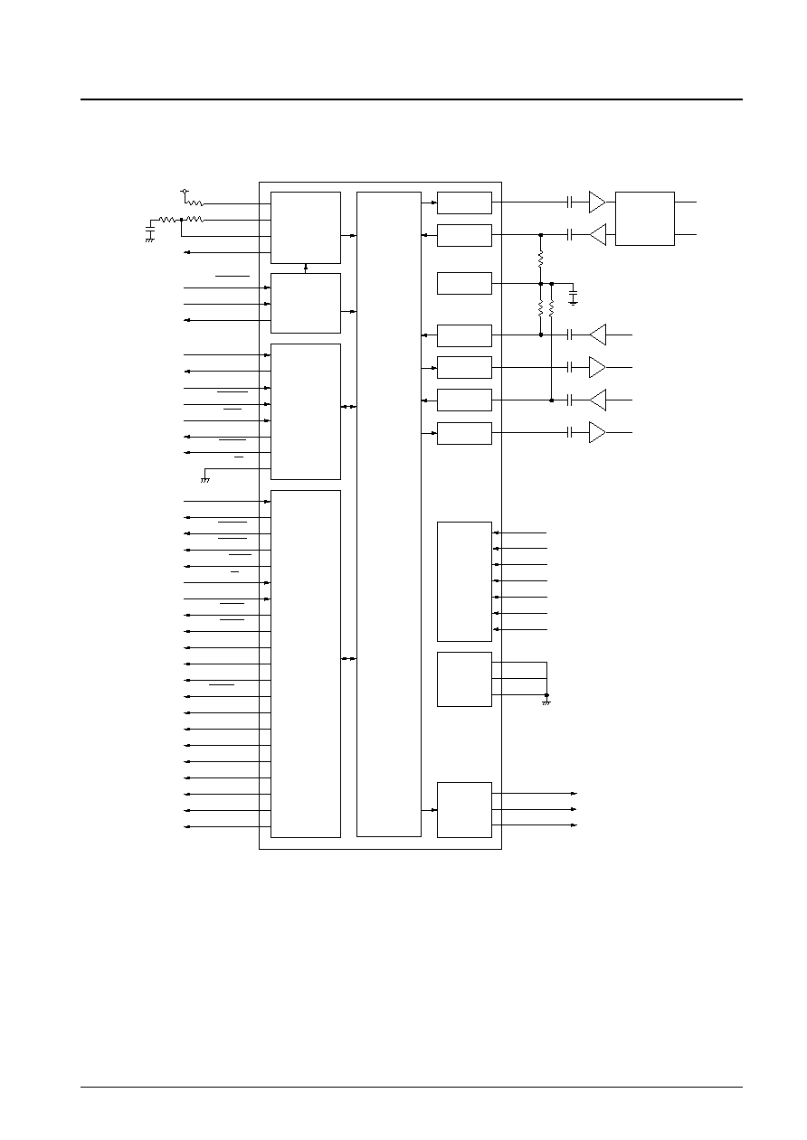
System Block Diagram
The diagram below shows a circuit that uses serial mode for the host CPU interface.
No. 6237-4/7
LC85050
+3.3VD
RIN
TXA
RXA
VERF
MIC
SPOUT
AXUI
AXUO
DV
DD
5
DV
DD
3
DGND
PV
DD
PGND
AV
DD
AGND
TESTR
TESTEN
TESTD
DSP
(FAVOR-11)
PLLO
PLLI
PLOCK
RESET
XIN
XOUT
DIN
DOUT
DCK
DSET
CS
BUSY
IREQ
P/S
MD0/MDI
MD1/MDO
MCS0
MCS1
SK/MRE
R/B0
R/B1
WP0
WP1
PA0
PA1
PA2
MWE/PA3
ALE/PA4
CLE/PA5
MD2/PA6
MD3/PA7
MD4/PA8
MD5/PA9
MD6/PA10
MA7/PA11
PLL frequency
multiplier
Timing
generator
Host CPU
interface
Memory
interface
D/A
converter
A/D
converter
Reference
voltage supply
A/D
converter
D/A
converter
A/D
converter
D/A
converter
Hybrid circuit
Power
supply
Test circuit
Monitor
output
circuit
Telephone line
Microphone
Speaker
Auxiliary analog input
Auxiliary analog output
No. 6237-5/7
LC85050
Pin Functions
Type
I
Input
B
Bidirectional
NC
Not connected
O
Output
P
Power supply
Pin No.
Pin
I/O
Function
1
PV
DD
P
PLL frequency multiplier 3.3 V power supply
2
PGND
P
PLL frequency multiplier ground
3
RIN
I
PLL frequency multiplier bias input
4
PLLI
I
PLL frequency multiplier VCO input
5
PLLO
O
PLL frequency multiplier charge pump output
6
PLOCK
O
PLL frequency multiplier operating status output
7
TESTR
I
8
TESTEN
I
Test inputs. These input must be connected to DGND during normal operation.
9
TESTD
I
10
RESET
I
Reset input
11
XIN
I
Oscillator amplifier input (3.6864 MHz)
12
XOUT
O
Oscillator amplifier output
13
DGND
P
Digital system ground
14
DV
DD
3
P
Digital system 3.3 V power supply
15
P/S
I
Host CPU interface selection signal
16
CPUCS
I
Host CPU chip select signal
17
CPUOE/DCK
I
In parallel mode: host CPU read signal
In serial mode: data clock input signal
18
CPUWE/DSET
I
In parallel mode: host CPU write signal
In serial mode: data transfer complete input
19
CD0/DIN
B
In parallel mode: host CPU data bus lines
20
CD1/DOUT
B
In serial mode: CD0 functions as host CPU serial data signal,
21
CD2
B
and CD1 functions as the host CPU serial data output.
22
CD3
B
23
DGND
P
Digital system ground
24
DV
DD
5
P
Digital system 5.0 V power supply
25
CD4
B
26
CD5
B
In parallel mode: host CPU data bus lines
27
CD6
B
28
CD7
B
29
BUSY
O
Status output that indicates the host CPU interface status
30
IREQ
O
Interrupt request output
31
DV
DD
3
P
Digital system 3.3 V power supply
32
DGND
P
Digital system ground
33
NC
34
NC
35
NC
36
PA0
O
37
PA1
O
Output ports
38
PA2
O
39
DV
DD
5
P
Digital system 5.0 V power supply
40
DGND
P
Digital system ground
41
AV
DD
P
Analog system 3.3 V power supply
42
AGND
P
Analog system ground
43
AUXI
I
Auxiliary analog input
44
MIC
I
Analog audio input
45
RXA
I
Analog circuit input
46
VREF
O
Analog reference output
47
AUXO
O
Auxiliary analog output
48
SPOUT
O
Analog audio output
49
TXA
O
Analog circuit output
50
AGND
P
Analog system ground
Continued on next page.