 | –≠–ª–µ–∫—Ç—Ä–æ–Ω–Ω—ã–π –∫–æ–º–ø–æ–Ω–µ–Ω—Ç: LC865612A | –°–∫–∞—á–∞—Ç—å:  PDF PDF  ZIP ZIP |
91400 RM (IM) HK No.6698-1/20
Ver.2.02
22599
Preliminary
Overview
The LC865632A/28A/24A/20A/16A/12A/08A microcontrollers are 8-bit single chip microcontrollers with the following
on-chip functional blocks :
- CPU : Operable at a minimum bus cycle time of 0.5µs (microsecond)
- On-chip ROM maximum capacity : 32K bytes
- On-chip RAM capacity : 640 bytes (LC865632A/28A/24A)
: 512 bytes (LC865620A/16A/12A/08A)
- 16-bit timer/counter (or two 8-bit timers)
- 16-bit timer/ PWM (or two 8-bit timers)
- 8-channel
◊
8-bit AD converter
- Two 8-bit synchronous serial-interface circuits
- 13-source 10-vectored interrupt system
All of the above functions are fabricated on a single chip.
Features
(1) Read Only Memory (ROM)
: LC865632A
32512
◊
8 bits
:
LC865628A
28672
◊
8 bits
:
LC865624A
24576
◊
8 bits
:
LC865620A
20480
◊
8 bits
:
LC865616A
16384
◊
8 bits
:
LC865612A
12288
◊
8 bits
:
LC865608A
8192
◊
8 bits
(2) Random Access Memory (RAM)
: LC865632A/28A/24A
640
◊
8 bits
:
LC865620A/16A/12A/08A
512
◊
8 bits
(3) Bus Cycle Time / Instruction Cycle Time
The LC865632A/28A/24A/20A/16A/12A/08A are constructed to read ROM twice within one instruction cycle. It has
1.7 times more performance capability within the same instruction cycle compared to our 4-bit microcontrollers
(LC66000 series).
Bus cycle time indicates the speed to read ROM.
Bus cycle time
cycle time
System clock oscillation
Oscillation Frequency
Voltage
0.5
µ
s 1.0
µ
s
Ceramic resonator oscillation
6MHz
4.5 - 6.0V
2.0
µ
s 4.0
µ
s
Ceramic resonator oscillation
1.5MHz
2.5 - 6.0V
3.75
µ
s 7.5
µ
s
RC resonator oscillation
800MHZ
2.5 - 6.0V
91.5
µ
s 183
µ
s
Crystal oscillation
32.568kHz
2.5 - 6.0V
8-Bit Single Chip Microcontroller
LC865632/28/24/20/16/12/08A
Ordering number : ENN*6698
CMOS IC

LC865632/28/24/20/16/12/08A
No.6698-2/20
(4) Ports
- Input / output ports
: 6 ports (42 terminals)
Input/output port programmable in nibble units
: 1 port (8 terminals)
(When the N-channel open drain output is selected, the data in a bit can be inputted.)
Input/output port programmable in a bit
: 5 ports (34 terminals)
Include 15V withstand N-channel open drain output port
: 3 ports (18 terminals)
- Input ports
: 2 ports (13 terminals)
(5) AD converter
- 8 channels
◊
8-bit AD converters
(6) Serial-interface
- Two 8-bit serial-interface circuits
LSB first / MSB first function available
- Internal 8-bit baud-rate generator in common with two serial-interface circuits
(7) Timers
- Timer0
16-bit timer / counter
2-bit prescaler + 8-bit programmable prescaler
Mode 0 : Two 8-bit timers with programmable prescaler
Mode 1 : 8-bit timer with a programmable prescaler + 8-bit counter
Mode 2 : 16-bit timer with a programmable prescaler
Mode 3 : 16-bit counter
The resolution of Timer is 1 tCYC. (tCYC : cycle time)
- Timer 1
16-bit timer / PWM
Mode 0 : Two 8-bit timers
Mode 1 : 8-bit timer + 8-bit PWM
Mode 2 : 16-bit timer
Mode 3 : Variable-bit PWM (9-16 bits)
In Mode 0 and Mode 1, the resolution of Timer and PWM is tCYC.
In Mode 2 and Mode 3, the resolution of Timer and PWM selectable ; tCYC or 1/2tCYC by program
- Base timer
Every 500ms overflow system for a clock application (using 32.568kHz crystal oscillation for Base timer clock)
Every 976
µ
s, 3.9ms, 15.6ms, 62.5ms overflow system (using 32.568kHz crystal oscillation for Base timer clock)
The Base timer clock selectable ; 32.568kHz crystal oscillation, System clock, and programmable prescaler output of
Timer 0
(8) Buzzer output
- The Buzzer sound frequency selectable ; 4KHz, 2KHz (using 32.568kHz crystal oscillation for Base timer clock)
(9) Remote control receiver circuit (Shares with the P73/INT3/T0IN terminal)
- Noise rejection function
- Switch polarity function
(10) Watchdog timer
- The watchdog timer is taken on RC outside
- Watchdog timer operation selectable : interrupt system, system reset

LC865632/28/24/20/16/12/08A
No.6698-3/20
(11) Interrupts system
- 13-sources 10-vectored interrupts :
1. External interrupt INT0 (include watchdog timer)
2. External interrupt INT1
3. External interrupt INT2, timer / counter T0L (Lower 8 bits)
4. External interrupt INT3, base timer
5. Timer / counter T0H (Upper 8-bit)
6. Timer T1L, Timer T1H
7. Serial interface SIO0
8. Serial interface SIO1
9. AD converter
10. Port 0
- Built-in interrupt priority control register
Microcontroller allows 3 levels of interrupt; low level, high level, and highest level of multiplex interrupt. It can specify
a low level or a high level interrupt priority from INT2/T0L through port 0 (i.e. the above interrupt number from three
through ten). It can also specify a low level or the highest level interrupt priority to INT0 and INT1.
(12) Real-time service operation
The Real-Time Service (RTS) functions the 4-byte data-transfer between the Special Function Registers at acknowledging
the interrupt request.
The RTS starts within 1 instruction cycle-time and completes within 5 instructions cycle-time after occurring the interrupt
request.
(13) Sub-routine stack levels
- 128 levels (Max.) : stack area included in RAM area
(14) Multiplication and division
- 16 bits
◊
8-bit (7 instruction cycle times)
- 16 bits ˜ 8-bit (7 instruction cycle times)
(15) Three oscillation circuits
- On-chip RC oscillation circuit using for the system clock
- On-chip CR oscillation circuit using for the system clock
- On-chip crystal oscillation circuit using for the system clock and for time-base clock
XT1 terminal can be used as P74
(16) Standby function
- HALT mode function
The HALT mode is used to reduce the power dissipation. In this operation mode, the program execution is stopped. This
operation mode can be released by the interrupt request signals or the initial system reset request signal.
- HOLD mode function
The HOLD mode is used to freeze all the oscillations ;
RC (internal), CF and Crystal oscillations. This mode can be released by the following operations.
∑ Reset terminal ( RES ) set to low level
∑ P70/INT0, P71/INT1 terminals set to assigned level (programmable)
∑ Input a Port 0 interrupt condition
(17) Factory shipment
∑ DIP64S, QFP64E delivery form
(18) Development support tools
- Evaluation (EVA) chip
: LC866098
- EPROM version
: LC86E5632
- One time version
: LC86P5632
- Emulator
: EVA86000 + ECB866600 (Evaluation chip board)
+ POD865000 (Pod for DIP64S)
+ POD865010 (Pod for QFP64E)
LC865632/28/24/20/16/12/08A
No.6698-4/20
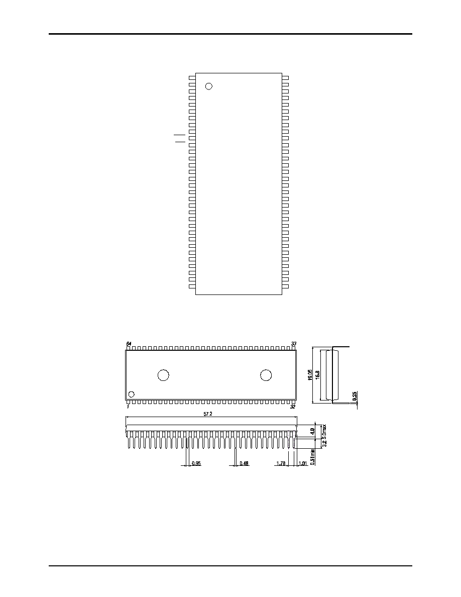
Pin Assignment
∑DIP64S
Package Dimension
(unit : mm)
3071
SANYO : DIP-64S(750mil)
P10/SO0
P11/SI0/SB0
P12/SCK0
P13/SO1
P14/SI1/SB1
P15/SCK1
P16/BUZ
P17/PWM
TEST1
RES
XT1/P74
XT2
VSS
CF1
CF2
VDD
P80/AN0
P81/AN1
P82/AN2
P83/AN3
P84/AN4
P85/AN5
P86/AN6
P87/AN7
P70/INT0
P71/INT1
P72/INT2/T0IN
P73/INT3/T0IN
P30
P31
P32
P33
1
2
3
4
5
6
7
8
9
10
11
12
13
14
15
16
17
18
19
20
21
22
23
24
25
26
27
28
29
30
31
32
64
63
62
61
60
59
58
57
56
55
54
53
52
51
50
49
48
47
46
45
44
43
42
41
40
39
38
37
36
35
34
33
P07
P06
P05
P04
P03
P02
P01
P00
P27
P26
P25
P24
P23
P22
P21
P20
VDDVPP
VSS
P51
P50
P47
P46
P45
P44
P43
P42
P41
P40
P37
P36
P35
P34
LC865632/28/24/20/16/12/08A
No.6698-5/20
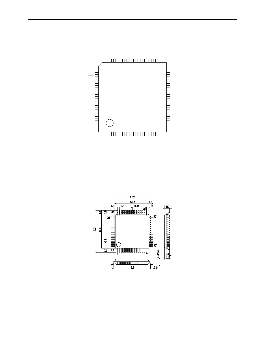
∑QIP64E
Package Dimension
(unit : mm)
3159
SANYO : QIP-64E
TEST1
RES
XT1/P74
XT2
VSS
CF1
CF2
VDD
P80/AN0
P81/AN1
P82/AN2
P83/AN3
P84/AN4
P85/AN5
P86/AN6
P87/AN7
49
50
51
52
53
54
55
56
57
58
59
60
61
62
63
64
32
31
30
29
28
27
26
25
24
23
22
21
20
19
18
17
P27
P26
P25
P24
P23
P22
P21
P20
VDDVPP
VSS
P51
P50
P47
P46
P45
P44
1
2
3
4
5
6
7
8
9
10
11
12
13
14
15
16
48
47
46
45
44
43
42
41
40
39
38
37
36
35
34
33
P
70/I
N
T
0
P
71/I
N
T
1
P
72/I
N
T
2/T
0
I
N
P
73/I
N
T
3/T
0
I
N
P3
0
P3
1
P3
2
P3
3
P3
4
P3
5
P3
6
P3
7
P4
0
P4
1
P4
2
P4
3
P
17/P
W
M
P
16/B
U
Z
P
15/S
C
K
1
P
14/S
I
1/S
B
1
P
13/S
O
1
P
12/S
C
K
0
P
11/S
I
0/S
B
0
P
10/S
O
0
P0
7
P0
6
P0
5
P0
4
P0
3
P0
2
P0
1
P0
0