 | –≠–ª–µ–∫—Ç—Ä–æ–Ω–Ω—ã–π –∫–æ–º–ø–æ–Ω–µ–Ω—Ç: LC867240A | –°–∫–∞—á–∞—Ç—å:  PDF PDF  ZIP ZIP |
91400 RM (IM) SK No.6702-1/20
Ver.1.03
10798
Preliminary
Overview
The LC867248A/40A/32A/24A microcontrollers are 8-bit single chip microcontrollers with the following on-chip
functional blocks :
- CPU : Operable at a minimum bus cycle time of 0.5
µ
s (microsecond)
- On-chip ROM maximum capacity : 48K bytes
- On-chip RAM capacity : 1152 bytes
- LCD controller/driver
- Two 16-bit timers (or four 8-bit timers)
- 8-channel
◊
8-bit AD converter
- Two 8-bit synchronous serial-interface circuits
- 13-source 10-vectored interrupt system
All of the above functions are fabricated on a single chip.
Features
(1) Read Only Memory (ROM)
: LC867248A
49152
◊
8 bits
:
LC867240A
40960
◊
8 bits
:
LC867232A
32768
◊
8 bits
:
LC867224A
24576
◊
8 bits
(2) Random Access Memory (RAM)
: 1152
◊
8 bits
(3) Bus Cycle Time/Instruction Cycle Time
Bus cycle time
cycle time
Clock divider
System clock oscillation
Oscillation Frequency
Voltage
0.5
µ
s 1.0
µ
s
1/1
Ceramic resonator oscillation
6MHz
4.5 - 6.0V
2
µ
s 4.0
µ
s
1/2
Ceramic resonator oscillation
3MHz
2.5 - 6.0V
7.5
µ
s 15.0
µ
s
1/2
RC resonator oscillation
800kHZ
2.5 - 6.0V
183
µ
s 366
µ
s
1/2
Crystal oscillation
32.768kHz
2.5 - 6.0V
8-Bit Single Chip Microcontroller
LC867248A/40A/32A/24A
Ordering number : ENN*6702
CMOS IC

LC867248A/40A/32A/24A
No.6702-2/20
(4) Ports
- Input / output ports
: 70 terminals (normal ports P0, P1, P3, PA, PB, PC, PD, PE, PF)
∑ P0
Input/output port programmable in nibble units
: 1 port (8 terminals)
(When the N-channel open drain output is selected, the data in a bit can be inputted.)
∑ P1
Input/output port programmable in a bit
: 1 port (8 terminals)
∑ P3
Input/output port programmable in a bit
: 1 port (6 terminals)
∑ PA, PB, PC, PD, PE, PF (can be used for LCD)
Input/output port programmable in two bits
: 6 ports (48 terminals)
- Input ports
: 21 terminals (P7, P8, PL)
- LCD control port
: 52 terminals
Segment output port
: 48 terminals
Common output port
: 4 terminals
(5) LCD controller / driver
- Selectable seven kinds of display mode (a combination of static 1/2, 1/3, 1/4 duty and 1/2, 1/3 bits)
- The segment and common output ports can be switched to a general input/output port.
(6) AD converter
- 8-channel
◊
8-bit AD converter
(7) Serial-interface
- One channel
◊
16-bit serial-interface circuits (8-bit transmission available by program)
- LSB first/MSB first function available
- Internal 8-bit baud-rate generator in common with two serial-interface circuits
(8) Timers
- Timer0
16-bit timer / counter
2-bit prescaler + 8-bit programmable prescaler
Mode 0 : Two 8-bit timers with programmable prescaler
Mode 1 : 8-bit timer with programmable prescaler + 8-bit counter
Mode 2 : 16-bit timer with programmable prescaler
Mode 3 : 16-bit counter
The resolution of Timer is tCYC. (tCYC : cycle time)
- Timer1
16-bit timer / PWM
Mode 0 : Two 8-bit timers
Mode 1 : 8-bit timer + 8-bit PWM
Mode 2 : 16-bit timer
Mode 3 : Variable-bit PWM (9-16 bits)
In Mode 0 and Mode 1, the resolution of Timer and PWM is tCYC.
In Mode 2 and Mode 3, the resolution of Timer and PWM selectable ; tCYC or 1/2tCYC by program
- Base timer
Every 500ms overflow system for a clock application (using 32.768kHz crystal oscillation for Base timer clock)
Every 976
µ
s, 3.9ms, 15.6ms, 62.5ms overflow system (using 32.768kHz crystal oscillation for Base timer clock)
The Base timer clock selectable ; 32.768kHz crystal oscillation, System clock, and programmable prescaler output of
Timer 0
(9) Buzzer output
- The Buzzer sound frequency selectable ; 4KHz, 2KHz (using 32.768kHz crystal oscillation for Base timer clock)

LC867248A/40A/32A/24A
No.6702-3/20
(10) Remote control receiver circuit (Shares with the P73/INT3/T0IN terminal)
- Noise rejection
- Switch polarity function
(11) Watchdog timer
- The watchdog timer is taken on RC outside
- Watchdog timer operation selectable : interrupt system, system reset
(12) Interrupts system
- 13-source 10-vectored interrupts :
1. External interrupt INT0 (include watchdog timer)
2. External interrupt INT1
3. External interrupt INT2, timer / counter T0L (Lower 8-bit)
4. External interrupt INT3, base timer
5. Timer / counter T0H (Upper 8-bit)
6. Timer T1L, Timer T1H
7. Serial interface SIO0
8. Serial interface SIO1
9. AD converter
10. Port 0
- Built-in interrupt priority control register
Microcontroller allows 3 levels of interrupt; low level, high level, and highest level of multiplex interrupt. It can specify a low
level or a high level interrupt priority from INT2/T0L through port 0 (i.e. the above interrupt number from three through
ten). It can also specify a low level or the highest level interrupt priority to INT0 and INT1.
(13) Real-time service operation
The Real-time service (RTS) functions the 4-byte data-transfer between the special function registers at acknowledging the
interrupt request.
The RTS starts within 1 instruction cycle-time and completes within 5 instruction cycle-times after occurring the interrupt
request.
(14) Sub-routine stack levels
- 128 levels (Max.) : stack area included in RAM area
(15) Multiplication and division
- 16-bit
◊
8-bit (7 instruction cycle times)
- 16-bit ˜ 8-bit (7 instruction cycle times)
LC867248A/40A/32A/24A
No.6702-4/20
(16) Three oscillation circuits
- On-chip RC oscillation circuit using for the system clock
- On-chip CF oscillation circuit using for the system clock
- On-chip crystal oscillation circuit using for the system clock and for time-base clock
(17) Standby function
- HALT mode function
The HALT mode is used to reduce the power dissipation. In this operation mode, the program execution is stopped. This
operation mode can be released by the interrupt request signals or the system reset request signal.
- HOLD Mode function
The HOLD mode is used to freeze all the oscillations ;
RC (internal), CF and Crystal oscillations. This mode can be released by the following operations.
∑ Reset terminal ( RES ) set to low level.
∑ Input a assigned level to P70/INT0 or P71/INT1 terminal
∑ Input a Port0 interrupt condition
(18) Factory shipment
∑ QFP100E delivery form
(19) Development support tools
- Evaluation (EVA) chip
: LC866093
- EPROM version
: LC86E7248
- One time version
: LC86P7248
- Emulator
: EVA86000 + ECB867200 (Evaluation chip board) + POD866200 (Pod)
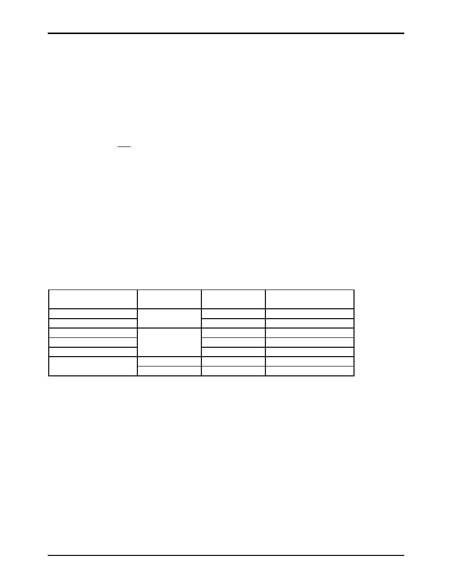
∑ Notes for use
Follow the under table
Frequency range
of the system clock
Voltage range
Clock Divider
Note
15kHz to 30kHz
1/1
Can not use 1/2 divider
30kHz to 6MHz
4.5V to 6.0V
1/1, 1/2
15kHz to 30kHz
1/1
Can not use 1/2 divider
30kHz to 1.5MHz
1/1, 1/2
1.5MHz to 3MHz
2.5V to 6.0V
1/2
Can not use 1/1 divider
4.5V to 6.0V
1/1, 1/2
Internal RC oscillation
2.5V to 6.0V
1/2
Can not use 1/1 divider
LC867248A/40A/32A/24A
No.6702-5/20
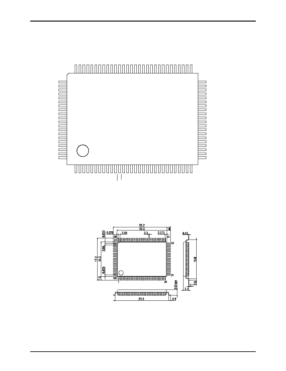
Pin Assignment
Package Dimension
(unit : mm)
3151
SANYO : QIP-100E
S20/PC4
S19/PC3
S18/PC2
S17/PC1
S16/PC0
S15/PB7
S14/PB6
S13/PB5
S12/PB4
S11/PB3
S10/PB2
S9/PB1
S8/PB0
S7/PA7
S6/PA6
S5/PA5
S4/PA4
S3/PA3
S2/PA2
S1/PA1
V2/PL5
V1/PL4
COM0/PL0
COM1/PL1
COM2/PL2
COM3/PL3
P30
P31
VSS3
VDD3
P32
P33
P34
P35
P00
P01
P02
P03
P04
P05
V3
/
P
L
6
S
47/PF7
S
46/PF6
S
45/PF5
S
44/PF4
S
43/PF3
S
42/PF2
S
41/PF1
S
40/PF0
S
39/PE
7
S
38/PE
6
S
37/PE
5
S
36/PE
4
S
35/PE
3
S
34/PE
2
S
33/PE
1
S
32/PE
0
S
31/PD
7
S
30/PD
6
S
29/PD
5
S
28/PD
4
S
27/PD
3
S
26/PD
2
VS
S2
VD
D
2
S
25/PD
1
S
24/PD
0
S
23/PC
7
S
22/PC
6
S
21/PC
5
P06 P07
P10/S
O
0
P11/S
I
0
/
SB
0
P12/S
C
K
0
P13/S
O
1
P14/S
I
1
/
SB
1
P15/S
C
K
1
P16/B
U
Z
P17/PW
M
0
P70/I
N
T
0
RE
S
XT
1/
P7
4
XT
2/
P75
VS
S1
CF1 CF2
VD
D
1
P80/A
N
0
P81/A
N
1
P82/A
N
2
P83/A
N
3
P84/A
N
4
P85/A
N
5
P86/A
N
6
P87/A
N
7
P71/I
N
T
1
P72/I
N
T
2
/T
0I
N
P73/I
N
T
3
/T
0I
N
S0
/
P
A
0
81
82
83
84
85
86
87
88
89
90
91
92
93
94
95
96
97
98
99
100
50
49
48
47
46
45
44
43
42
41
40
39
38
37
36
35
34
33
32
31
1 2 3 4 5 6 7 8 9 10 11 12 13 14 15 16 17 18 19 20 21 22 23 24 25 26 27 28 29 30
80 79 78 77 76 75 74 73 72 71 70 69 68 67 66 65 64 63 62 61 60 59 58 57 56 55 54 53 52 51