 | –≠–ª–µ–∫—Ç—Ä–æ–Ω–Ω—ã–π –∫–æ–º–ø–æ–Ω–µ–Ω—Ç: LC868008A | –°–∫–∞—á–∞—Ç—å:  PDF PDF  ZIP ZIP |
91400 RM (IM) HO No.6723-1/28
Ver.1.12
61298
Preliminary
Overview
The LC868016A/12A/08A microcontrollers are 8-bit single chip microcontrollers with the following on-chip functional
blocks :
- CPU : Operable at a minimum bus cycle time of 0.5
µ
s (microseconds)
- On-chip ROM maximum capacity : 16K bytes
- On-chip RAM capacity : 640 bytes
- Dot-matrix liquid crystal display (LCD) automatic display controller / driver
- External memory
- 16-bit timer / counter (or two 8-bit timers)
- 16-bit timer / PWM (or two 8-bit timers)
- Two 8-bit synchronous serial-interface circuits
- 13-source 9-vectored interrupt system
All of the above functions are fabricated on a single chip.
8-Bit Single Chip Microcontroller with
16/12/08K-Byte ROM and 640-Byte RAM On Chip
LC868016/12/08A
Ordering number : ENN*6723
CMOS IC
LC868016/12/08A
No.6723-2/28
Features
(1) Read Only Memory (ROM)
: LC868016A
16384
◊
8 bits
:
LC868012A
12288
◊
8 bits
:
LC868008A
8192
◊
8 bits
(2) Random Access Memory (RAM)
: 512
◊
8 bits (calculation area)
128
◊
8 bits (display area)
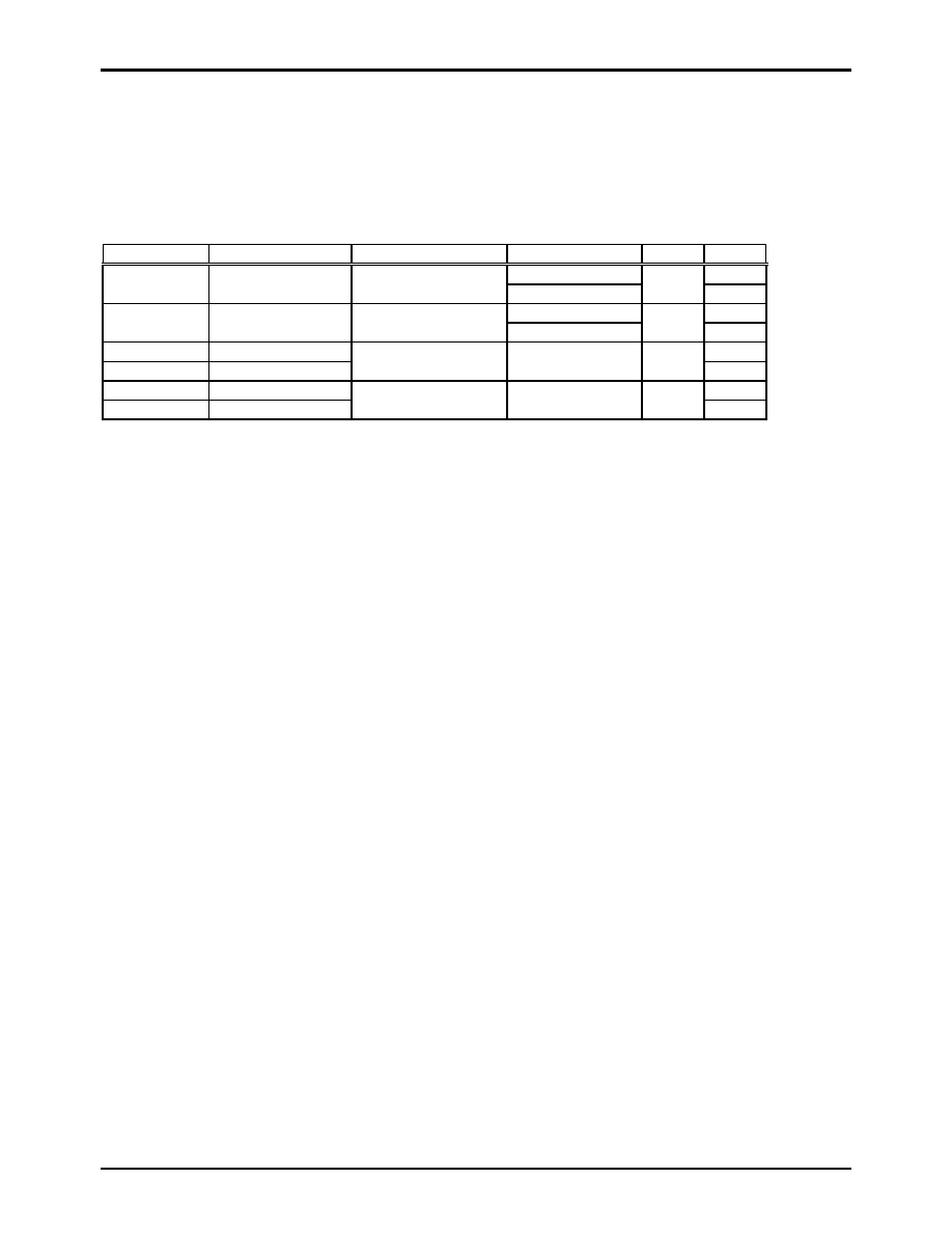
(3) Bus Cycle Time / Instruction Cycle Time
Bus cycle time
Instruction cycle time
System clock oscillation
Oscillation frequency
Voltage
Note
12MHz OCR7=0
0.5
µ
s 1
µ
s Ceramic
(CF)
6MHz
4.5-6.0V
OCR7=1
3MHz OCR7=0
2.0
µ
s 4
µ
s Ceramic
(CF)
1.5MHz
2.5-6.0V
OCR7=1
7.5
µ
s 15
µ
s OCR7=0
3.8
µ
s 7.5µs
Internal RC
800kHz
2.5-6.0V
OCR7=1
183
µ
s 366
µ
s OCR7=0
91.5 183
µ
s
Crystal (XTAL)
32.768kHz
2.5-6.0V
OCR7=1
* Bus cycle time means ROM-read period.
OCR7 : Bit-7 of the oscillation control register.
(4) Ports
- Input / output ports
: 6 ports (47 terminals)
Input/output port programmable in a nibble
: 1 port (8 terminals)
Input/output port programmable every function unit : 1 port (7 terminals)
Input/output port programmable in a bit
: 4 ports (32 terminals)
- Input port
: 1 port (4 terminals)
- Ports at external memory mode
1. External Latch
Port 0 : Address output of lower 8-bit, input/output of data
Port 2 : Address output of upper 8-bit
Port 5 : Bank address output
2. No External Latch
Port 0 : Input/output of data
Port 3 : Address output of lower 8-bit
Port 2 : Address output of upper 8-bit
Port 5 : Bank address output
(Set whether the external latch is used or not by program.)
- LCD segment driver output ports
: 48 terminals
(Function change available : segment/common)
- LCD common driver output ports
: 16 terminals
(1/64 duty maximum : at using segment output ports as common output by mask option)
(5) External memory access
- External program memory access function
External program memory capacity : 64K bytes
Programable switch internal program/external program
(At initial : Internal program)
Enable/disable control of external program --> internal program memory switch

LC868016/12/08A
No.6723-3/28
Ports
Port 2 : Address output of upper 8-bit
Uses EROE terminal ( OE signal of the external ROM)
1. Using the external latch
Port 0 : Address output of lower 8-bit, data input port
Uses the ADLC terminal (latch clock of the lower 8-bit address signal)
2. Not use the external latch
Port 0 : Input port of data
Port 3 : Address output of lower 8-bit
- External data memory access function
Using the LDC instruction
External memory capacity : 16M bytes
1. Internal program memory
Switch the reference of internal ROM data/external ROM data by program.
2. External program memory
Reference external ROM data only.
Ports
Port 2 : Address output of upper 8-bit
Port 5 : Bank address output
Uses
EROE terminal ( OE signal of the external ROM)
1. Using external latch
Port 0 : Address output of lower 8-bit, input port of data
Uses the ADLC terminal (latch clock of the lower 8-bit address signal)
2. Not use external latch
Port 0 : Input port of data
Port 3 : Address output of lower 8-bit
- External RAM memory access function
Using the LDX, STX instruction
External memory capacity : 16M bytes
Ports
Port 2 : Address output of upper 8-bit
Port 5 : Bank address output
Uses the P46 terminal ( OE signal of external RAM) : the LDX instruction execution
Uses the P47 terminal ( WE signal of external RAM) : the STX instruction execution
1. Using the external latch circuit
Port 0 : Address output of lower 8-bit, input/output port of data
Uses the ADLC terminal (latch clock of the lower 8-bit address signal)
2. Not use the external latch circuit
Port 0 : Input/output port of data
Port 3 : Address output of lower 8-bit
(6) LCD automatic display controller
- Display duty
: 1/1 - 1/64 duty
- Display bias
: 1/4, 1/5, 1/7, 1/9 bias
- Programmable character display / graphic display
- Character display
1. On-chip character generator ROM
ROM capacity
: 8960 bits
Character font
: 5
◊
7 dots
Number of Characters
: 256
2. LCD instruction
Display
:
ON/OFF
Cursor
:
ON/OFF/BLINK
Character blink
: ON/OFF
Character scroll
: Control by specified starting address
LC868016/12/08A
No.6723-4/28
- Graphic display
LC868000 series
: 1024 dots Maximum
External segment driver : Enable to extend of LCD drive
- LCD contrast
LCD display contrast programmable
- LCD display power supply
Doubler/Tripler circuit programmable
Doubler voltage in the tripler mode must not be used for LCD display power supply
If doubler voltage is used for LCD display power supply, the doubler mode must be selected by user program.
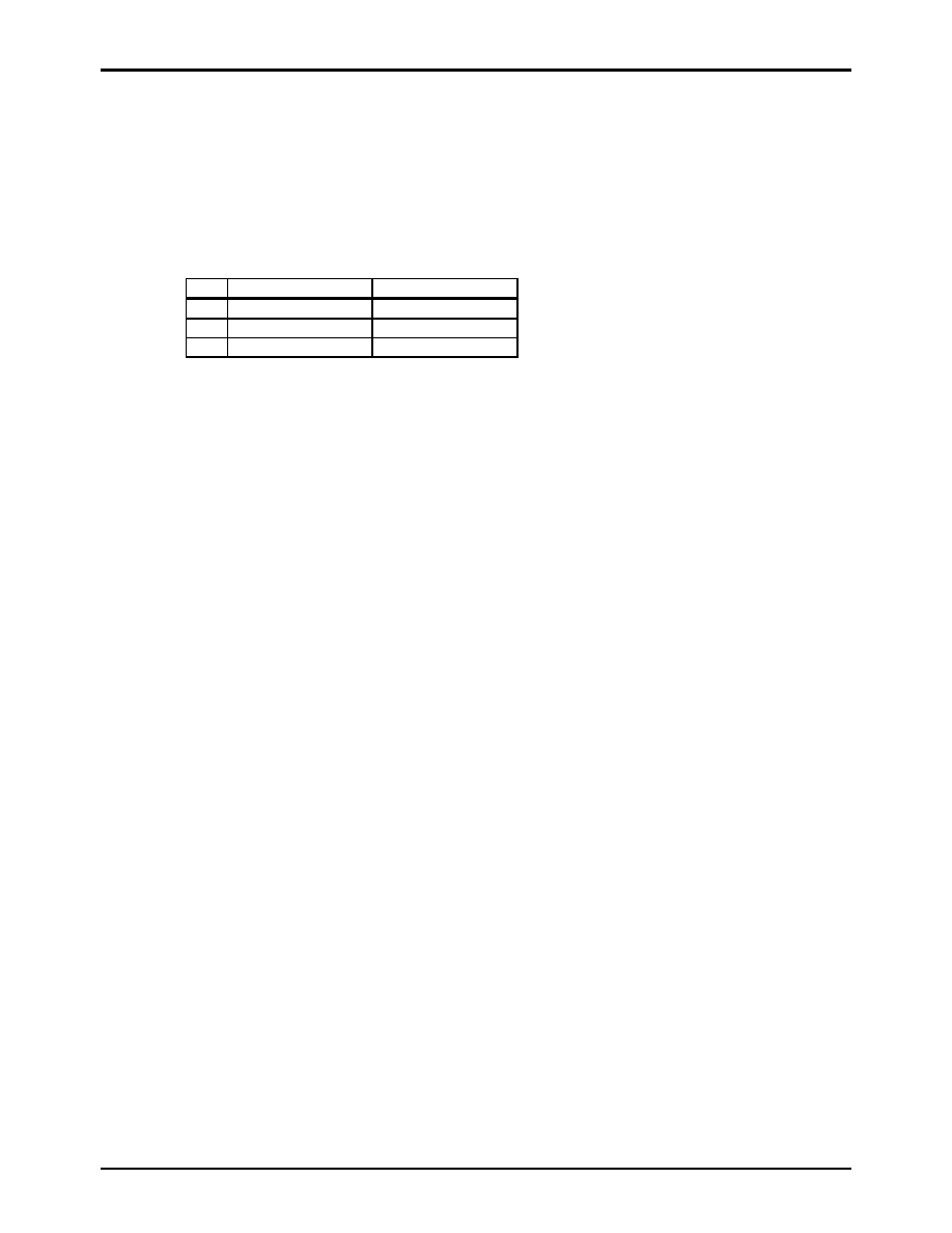
- LCD driver
Following three kinds of combination can be selected by mask option
No.
Segment output port
Common output port
1 48
16
2 32
32
3 0
64
(7) Serial-interface
- Two 8-bit serial-interface circuits
LSB first / MSB first function available
- Internal 8-bit baud-rate generator in common with two serial-interface circuits
(8) Timers
- Timer0 (T0L, T0H)
16-bit timer / counter
2-bit prescaler + 8-bit programmable prescaler
Mode 0 : Two 8-bit timers with programmable prescaler
Mode 1 : 8-bit timer with a programmable prescaler + 8-bit counter
Mode 2 : 16-bit timer with a programmable prescaler
Mode 3 : 16-bit counter
- Timer1 (T1L, T1H)
16-bit timer / PWM
Mode 0 : Two 8-bit timers
Mode 1 : 8-bit timer + 8-bit PWM
Mode 2 : 16-bit timer
Mode 3 : Variable-bit PWM (9-16 bits)
- Base timer
Every 500ms overflow system for a clock application (using 32.768kHz crystal oscillation for Base timer clock)
The Base timer clock selectable ; 32.768kHz crystal oscillation, System clock, and programmable prescaler output of
Timer 0
(9) Buzzer output
- The Buzzer sound frequency selectable ; 4KHz, 2KHz
(10) Remote control receiver circuit (using P73/INT3/T0IN terminal)
- Noise rejection available
- The interrupt polarity selectable
(11) Watchdog timer
- The watchdog timer is taken on RC outside. (using P70/INT0 terminal)
- Watchdog timer operation selectable : interrupt system, system reset

LC868016/12/08A
No.6723-5/28
(12) Interrupts system
- 13-source 9-vectored interrupts :
1. External interrupt INT0 (includes watchdog timer)
2. External interrupt INT1
3. External interrupt INT2, timer / counter T0L (timer 0 lower 8 bits)
4. External interrupt INT3, base timer
5. Timer / counter T0H (timer 0 upper 8-bit)
6. Timer T1L (timer 1 lower 8-bit), Timer T1H (timer 1 upper 8-bit)
7. Serial interface SIO0
8. Serial interface SIO1
9. Port 0 or Port 3
- Interrupt priority control available
Microcomputer allows 3 levels of interrupt; low level, high level, and highest level of multiplex interrupt. It can
specify a low level or a high level interrupt priority from INT2/T0L through port 0 or port 3 (the above interrupt
number from three through nine). It can also specify a low level or the highest level interrupt priority to INT0 and
INT1.
(13) Sub-routine stack levels
- 128 levels (Max.) : stack area included in RAM area
(14) Multiplication and division
- 16 bits
◊
8-bit (7 instruction cycle times)
- 16 bits / 8-bit (7 instruction cycle times)
(15) Three oscillation circuits
- On-chip RC oscillation circuit using for the system clock, for the LCD display and for the step-up circuit.
- On-chip CF oscillation circuit using for the system clock and for the LCD display.
- On-chip crystal oscillation circuit using for the system clock, for time-base clock and for the LCD display.
(16) Standby function
- HALT mode function
The HALT mode is used to reduce the power dissipation. In this operation mode, the program execution is stopped.
This operation mode can be released by the interrupt request signals or setting to low level for the reset terminal
( RES ).
- HOLD mode function
The HOLD mode is used to freeze all the oscillations ;
RC (internal), CF and Crystal oscillations. This mode can be released by the following operations:
∑ Reset terminal ( RES ) set to low level.
∑ Set to assigned level to INT0/1 terminals.
∑ Set to assigned level to Port 0/3.
(17) Factory shipment
- Chip
QIC160 package shipping available for sample evaluation.
(18) Development support tools
- Evaluation (EVA) chip
: LC868099
- Emulator
: EVA86000 + ECB868000 (Evaluation chip board)