 | –≠–ª–µ–∫—Ç—Ä–æ–Ω–Ω—ã–π –∫–æ–º–ø–æ–Ω–µ–Ω—Ç: LC86E6449 | –°–∫–∞—á–∞—Ç—å:  PDF PDF  ZIP ZIP |
91400 RM (IM) SK No.6746-1/22
Ver.1.04
73196
Preliminary
Overview
The LC86E6449 is a CMOS 8-bit single chip microcontroller with UVEPROM for the LC866400 series.
This microcontroller has the function and the pin description of the LC866400 series mask ROM version, and 48K-byte
EPROM. The program data is rewritable. It is suitable to develop the program.
Features
(1) Option switching by EPROM data
The option function of the LC866400 series can be specified by the EPROM data.
LC86E6449 can be checked the function of the trial pieces using the mass production board.
(2) Internal one-time EPROM capacity
: 49408 bytes
(3) Internal RAM capacity
: 1152 bytes
Used EPROM or RAM capacity are equal ROM or RAM capacity of mask ROM version which applies LC86E6449.
Mask ROM version
EPROM capacity
RAM capacity
LC866448 49152
bytes
1152
bytes
LC866444 45056
bytes
1152
bytes
LC866440 40960
bytes
1152
bytes
LC866436 36864
bytes
1152
bytes
LC866432 32768
bytes
768
bytes
LC866428 28672
bytes
768
bytes
LC866424 24576
bytes
768
bytes
LC866420 20480
bytes
640
bytes
LC866416 16384
bytes
640
bytes
LC866412 12288
bytes
512
bytes
LC866408
8192 bytes
512 bytes
8-Bit Single Chip Microcontroller
with the UVEPROM
LC86E6449
Ordering number : ENN*6746
CMOS IC

LC86E6449
No.6746-2/22
(4) Operating supply voltage
: 4.5V to 6.0V
(5) Instruction cycle time
: 1.0
µ
s to 366
µ
s
(6) Operating temperature
: +10
∞
C to +40
∞
C
(7) The pin compatible with the LC866400 series mask ROM devices
(8) Applicable mask ROM version
: LC866448/LC866444/LC866440/LC866436//LC866432/LC866428
/LC866424/LC866420/LC866416/LC866412/LC866408
(9) Operating temperature
: QFC80E (with window)
Notice for use
LC86E6449 is provided for the first release and small shipping of the LC866400 series.
At using, take notice of the followings.
(1) A point of difference LC86E6449 and LC866400 series
Item LC86E6449
LC866448/44/40/36/32/28/24/20/16/12/08
Operation after reset
releasing
The option is specified until 3ms after
going to a `H' level to the reset terminal
by dgrees. The program is executed
from 00H of the program counter.
The program is executed from 00H of the
program counter immediately after going to
a `H' level to reset terminal.
Pull-down resistor of
the following pins
∑S0/T0 ≠ S6/T6
∑S7/T7 ≠ S15/T15
∑S16 ≠ S27
∑S28 ≠ S37
Pull-down resistor
provided/not provided
Not provided
Provided (fixed)
Provided (fixed)
Not provided
Pull-down resistor
provided/not provided
Specified by the option
Provided (fixed)
Specified by the option
Specified by the option
Operating supply
Voltage range (VDD)
4.5V to 6.0V
2.5V to 6.0V
Operating temperature
range (Topg)
+10
∞
C
to +40
∞
C
-30
∞
C
to +70
∞
C
"L" level hold Tr. of the
high voltage withstand input
terminal
Power dissipation
Refer to `electrical characteristics' on the semiconductor news.
LC86E6449 uses 256 bytes that is addressed on FF00H to FFFFH in the program memory as the option configuration data
area. This option configuration cannot execute all options which LC866400 series have. Next tables show the options
that correspond and not correspond to LC86E6449.
LC86E6449
No.6746-3/22
∑ A kind of the option corresponding of the LC86E6449
A kind of option
Pins, Circuits
Contents of the option
1. N-channel open drain output
2. CMOS output
*1
Port 0
1. Pull-up MOS Tr. proveded
2. Pull-up MOS Tr. not provided
*2
Port 1
*1
1. Input
: Programmable pull-up MOS Tr.
Output : N-channel open drain
2. Input
: Programmable pull-up MOS Tr.
Output :
CMOS
Input/output form of
Input/output ports
Port 3
*1
1. Input
: No Programmable pull-up MOS Tr.
Output : N-channel open drain
2. Input
: Programmable pull-up MOS Tr.
Output : CMOS
Pull-up MOS Tr. of input ports
Port 7
*1
1. No Pull-up MOS Tr.
2. Pull-up MOS Tr.
*1) Specified in a bit
*2) Specified in nibble unit. The port of N-channel open drain output does not have the Pull-up MOS Tr..
∑ A kind of the option not corresponding of the LC86E6449
A kind of option
Pins, Circuits
LC86E6449
LC866448/44/40/36/32/28/24/20/16/12/08
Pull-down resistor of
the high voltage
Withstand output terminals
∑S0/T0 to S6/T6
∑S16 to S27
∑S28 to S37
Not provided
Provided (fixed)
Not provided
Specified by the option
Specified by the option
Specified by the option
(2) Option
The option data is created by the option specified program "SU86K.EXE". The created option data is linked to the
program area by linkage loader "L86K.EXE".
LC86E6449
No.6746-4/22
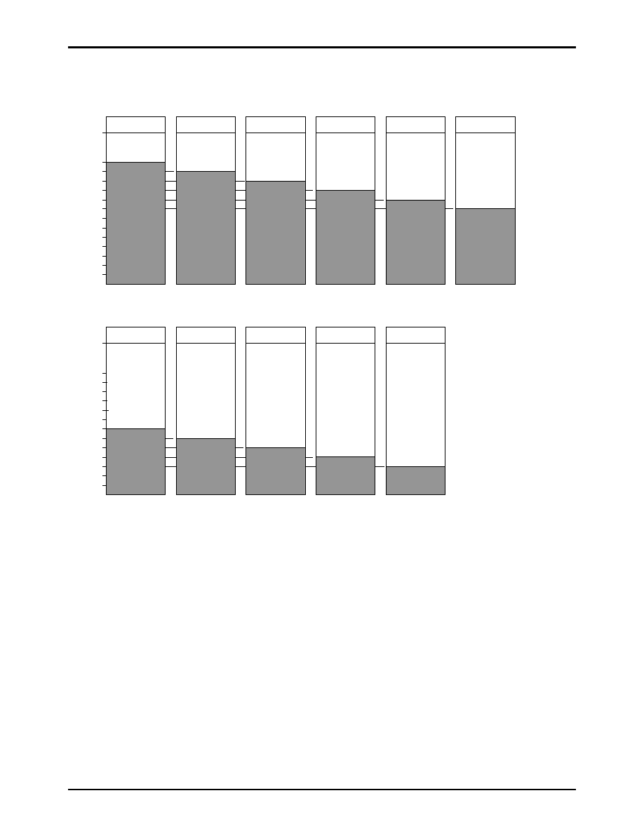
(3) ROM space
LC86E6449 and LC866400 series use 256 bytes that is addressed on 0FF00H to 0FFFFH in the program memory as the
option specified data area. These program memory capacity are 61440 bytes that is addressed on 0000H to BFFFH.
0FFFFH
0FF00H
0EFFFH
0DFFFH
0CFFFH
0BFFFH
0AFFFH
9FFFH
8FFFH
7FFFH
6FFFH
5FFFH
4FFFH
3FFFH
2FFFH
1FFFH
0FFFH
0000H
The option specified
area 256 bytes
Program area
48K bytes
LC866448
The option
specified area
Program area
44K bytes
LC866444
The option
specified area
Program area
40K bytes
LC866440
The option
specified area
Program area
36K bytes
LC866436
The option
specified area
Program area
32K bytes
LC866432
The option
specified area
Program area
28K bytes
LC866428
0FFFFH
0FF00H
0EFFFH
0DFFFH
0CFFFH
0BFFFH
0AFFFH
9FFFH
8FFFH
7FFFH
6FFFH
5FFFH
4FFFH
3FFFH
2FFFH
1FFFH
0FFFH
0000H
The option
specified area
Program area
24K bytes
LC866424
The option
specified area
Program area
20K bytes
LC866420
The option
specified area
Program area
16K bytes
LC866416
The option
specified area
Program area
12K bytes
LC866412
The option
specified area
Program area
8K bytes
LC866408
LC86E6449
No.6746-5/22
How to use
(1) Specification of option
Programming data for EPROM of the LC86E6449 is required.
Debugged evaluation file (EVA file) must be converted to an INTEL-HEX formatted file (HEX file) with file converter
program, EVA2HEX.EXE. The HEX file is used as the programming data for the LC86E6449.
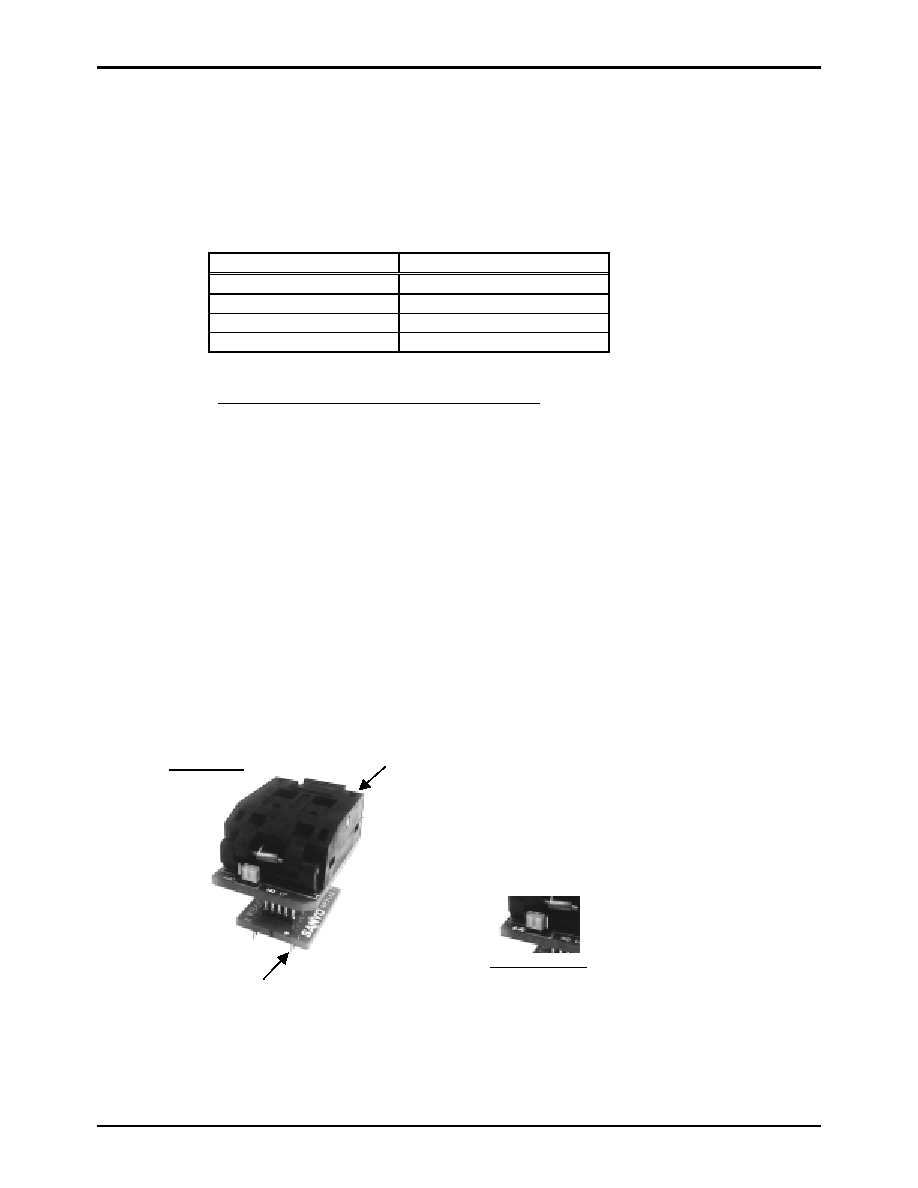
(2) How to program for the EPROM
LC86E6449 can be programmed by the EPROM programmer with attachment ; W86EP6448Q.
∑ Recommended EPROM programmer
Productor EEPROM
programmer
Advantest
R4945, R4944, R4943
Andou AF-9704
AVAL PKW-1100,
PKW-3000
Minato electronics
MODEL 1890A
∑ "27512 (Vpp=12.5V) Intel high speed programming" mode available. The address must be set to "0 to
0FFFFH" and a jumper (DASEC) must be set to `OFF' at programming.
(3) How to use the data security function
"Data security" is the disabled function to read the data of the EPROM.
The following is the process in order to execute the data security.
1. Set `ON' the jumper of attachment.
2. Program again. Then EPROM programmer displays the error. The error means normally activity of the data security.
It is not a trouble of the EPROM programmer or the LSI.
Notes
∑ Data security is not executed when the data of all address have `FFH' at the sequence 2 above.
∑ The programming by a sequential operation "BLANK
PROGRAM
VERIFY" cannot be executed data security at the
sequence 2 above.
∑ Set to `OFF' the jumper after executing the data security.
W86EP6448Q
Data security
1 pin
1 pin mark
of LSI
Not data security