91400 RM (IM) SK No.6749-1/19
Ver.1.02
80196
Preliminary
Overview
The LC86E7248 is a CMOS 8-bit single chip microcontroller with UVEPROM for the LC867200 series. This
microcontroller has the function and the pin description of the LC867200 series mask ROM version, and 48K-byte EPROM.
The program data is rewritable. It is suitable to develop the program.
Features
(1) Option switching by EPROM data
The option function of the LC867200 series can be specified by the EPROM data.
LC86E7248 can be checked the functions of the trial pieces using the mass production board.
(2) Internal EPROM capacity
: 49408 bytes
(3) Internal RAM capacity
: 1152 bytes
Used EPROM or RAM capacity are equal ROM or RAM capacity of mask ROM version which applies LC86E7248.
Mask ROM version
EPROM capacity
RAM capacity
LC867248
49152 bytes
1152 bytes
LC867240
40960 bytes
1152 bytes
LC867232
32768 bytes
1152 bytes
LC867224
24576 bytes
1152 bytes
(4) Operating supply voltage
: 4.5V to 6.0V
(5) Instruction cycle time
: 1
�
s to 366
�
s
(6) Operating temperature
: +10
�
C to +40
�
C
(7) The pin compatible with the LC867200 series mask ROM devices
(8) Applicable mask ROM version
: LC867248/40/32/24
(9) Factory shipment
: QFC100S (with window)
8-Bit Single Chip Microcontroller
with the UVEPROM
LC86E7248
Ordering number : ENN*6749
CMOS IC
LC86E7248
No.6749-2/19
Notice for use
At using, take notice of the followings.
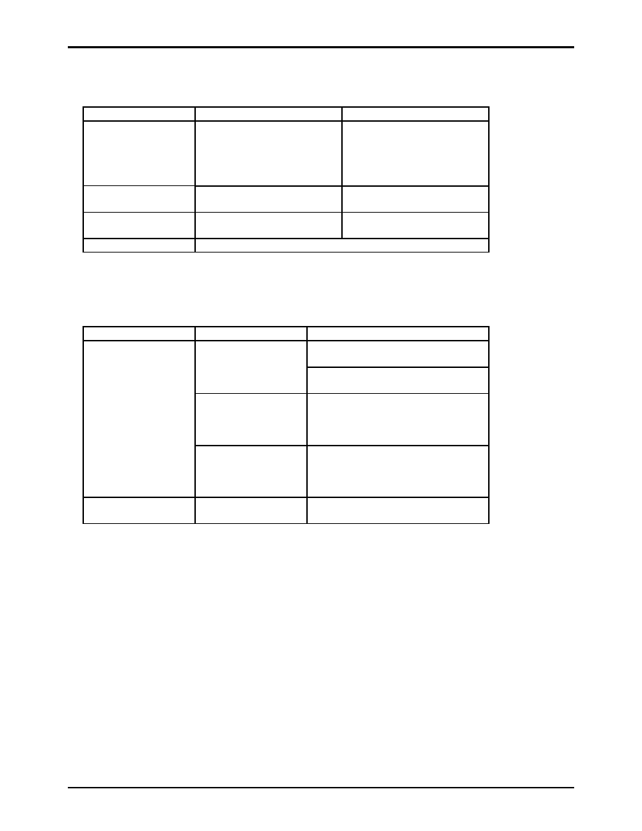
(1) A point of difference LC86E7248 and LC867200 series
Item LC86E7248
LC867248/40/32/24
Operation after reset
releasing
The option is specified until 3ms after
going to a `H' level to the reset
terminal by degrees. The program is
executed from 00H of the program
counter.
The program is executed from 00H of
the program counter immediately after
going to a `H' level to the reset
terminal.
Operating supply
voltage range (VDD)
4.5V to 6.0V
2.5V to 6.0V
Operating temperature
range (Topr)
+10
�
C to +40
�
C -30
�
C to +70
�
C
Power dessipation
Refer to `electrical characteristics' on the semiconductor news.
LC86E7248 uses 256 bytes that is addressed on 0FF00H to FFFFH in the program memory as the option configuration data
area. This option configuration cannot execute all options which LC867200 series have. Next tables show the options
that correspond and not correspond to LC86E7248.
� A kind of the option corresponding of the LC86E7248
A kind of option
Pins, Circuits
Contents of the option
1. N-channel open drain output
2. CMOS output
*1
Port 0
1. Pull-up MOS Tr.
2. No Pull-up MOS Tr.
*2
Port 1
*1
1. Input : Programmable pull-up MOS Tr.
Output : N-channel open drain
2. Input : Programmable pull-up MOS Tr.
Output : CMOS
Input/output form of
input/output ports
Port 3
*1
1. Input : No Programmable pull-up MOS Tr.
Output : N-channel open drain
2. Input : Programmable pull-up MOS Tr.
Output : CMOS
Pull-up MOS Tr. of
input port
Ports 70, 71, 72, 73
*1
1. No Pull-up MOS Tr.
2. Pull-up MOS Tr.
*1) Specified in a bit.
*2) Specified in nibble unit. Pull-up MOS Tr. is not provided in N-channel open drain output port.
The port operation related the option is different at reset. Refer to the next table.
LC86E7248
No.6749-3/19
(1) Option
The option data is created by the option specified program "SU86K.EXE". The created option data is linked to the
program area by linkage loader "L86K.EXE".
(2) ROM space
LC86E7248 and LC867200 series use 256 bytes that is addressed on 0FF00H to 0FFFFH in the program memory as the
option specified data area. These program memory capacity are 49152 bytes that is addressed on 0000H to 0BFFFH.
0FFFFH
0FF00H
0EFFFH
0DFFFH
0CFFFH
0BFFFH
0AFFFH
9FFFH
8FFFH
7FFFH
6FFFH
5FFFH
4FFFH
3FFFH
2FFFH
1FFFH
0FFFH
0000H
Option data
area 256 bytes
Program area
48K bytes
Option
data area
Program area
40K bytes
LC867248 LC867240
Option
data area
Program area
32K bytes
LC867232
Option
data area
LC867224
Program area
28K bytes
LC86E7248
No.6749-4/19
How to use
(1) Specification of option
Programming data for PROM of the LC86E7248 is required.
Debugged evaluation file (EVA file) must be converted to an INTEL-HEX formatted file (HEX file) with file converter
program, EVA2HEX.EXE. The HEX file is used as the programming data for the LC86P6548.
(2) How to program for the EPROM
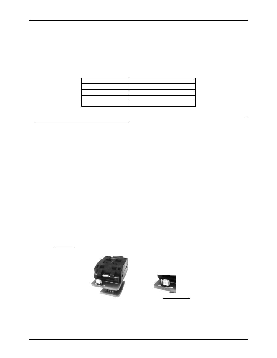
The LC86E7248 can be programmed by EPROM programmer with attachment ; W86EP7248Q
� Recommended EPROM programmer
Productor EPROM
programmer
Advantest
R4945, R4944, R4943
Andou AF-9704
AVAL PKW-1100,
PKW-3000
Minato electronics
MODEL1890A
� "27512 (Vpp=12.5V) Intel high speed programming" mode available. The address must be set to "0 to 0FFFFH" and a
jumper (DASEC) must be set to `OFF' at programming.
(3) How to use the data security function
"Data security" is the disabled function to read the data of the EPROM.
The following is the process in order to execute the data security.
1. Set `ON' the jumper of attachment.
2. Program again. Then EPROM programmer displays the error. The error means normally activity of the data
security. It is not a trouble of the EPROM programmer or the LSI.
Notes
� Data security is not executed when the data of all address have `FFH' at the sequence 2 above.
� The programming by a sequential operation "BLANK=>PROGRAM=>VERIFY" cannot be executed data security at the
sequence 2 above.
� Set to `OFF' the jumper after executing the data security.
(4) How to eliminate
The programming data can be erased by using the EPROM eraser.
(5) Shielding
The UVEPROM (ultraviolet erasable programmable ROM) is in it. Put the seal on the window in use.
W86EP7248Q
Data security
Not data security

LC86E7248
No.6749-5/19
Pin Assignment
SANYO : QFC100S
S20/PC4
S19/PC3
S18/PC2
S17/PC1
S16/PC0
S15/PB7
S14/PB6
S13/PB5
S12/PB4
S11/PB3
S10/PB2
S9/PB1
S8/PB0
S7/PA7
S6/PA6
S5/PA5
S4/PA4
S3/PA3
S2/PA2
S1/PA1
V2/PL5
V1/PL4
COM0/PL0
COM1/PL1
COM2/PL2
COM3/PL3
P30
P31
VSS3
VDD3
P32
P33
P34
P35
P00
P01
P02
P03
P04
P05
V3
/
P
L
6
S
47/PF7
S
46/PF6
S
45/PF5
S
44/PF4
S
43/PF3
S
42/PF2
S
41/PF1
S
40/PF0
S
39/PE
7
S
38/PE
6
S
37/PE
5
S
36/PE
4
S
35/PE
3
S
34/PE
2
S
33/PE
1
S
32/PE
0
S
31/PD
7
S
30/PD
6
S
29/PD
5
S
28/PD
4
S
27/PD
3
S
26/PD
2
VS
S2
VD
D
2
S
25/PD
1
S
24/PD
0
S
23/PC
7
S
22/PC
6
S
21/PC
5
P06 P07
P10/S
O
0
P11/S
I
0
/
SB
0
P12/S
C
K
0
P13/S
O
1
P14/S
I
1
/
SB
1
P15/S
C
K
1
P16/B
U
Z
P17/PW
M
0
P70/I
N
T
0
RE
S
XT
1/
P7
4
XT
2/
P
7
5
VS
S1
CF1 CF2
VD
D
1
P80/A
N
0
P81/A
N
1
P82/A
N
2
P83/A
N
3
P84/A
N
4
P85/A
N
5
P86/A
N
6
P87/A
N
7
P71/I
N
T
1
P72/I
N
T
2
/T
0I
N
P73/I
N
T
3
/T
0I
N
S0
/
P
A
0
81
82
83
84
85
86
87
88
89
90
91
92
93
94
95
96
97
98
99
100
50
49
48
47
46
45
44
43
42
41
40
39
38
37
36
35
34
33
32
31
1 2 3 4 5 6 7 8 9 10 11 12 13 14 15 16 17 18 19 20 21 22 23 24 25 26 27 28 29 30
80 79 78 77 76 75 74 73 72 71 70 69 68 67 66 65 64 63 62 61 60 59 58 57 56 55 54 53 52 51