91400 RM (IM) SK No.6712-1/24
Ver.1.04
61899
Preliminary
Overview
The LC87F72C8A is an 8 bit single chip microcontroller with the following on-chip functional blocks :
- CPU: operable at a minimum bus cycle time of 100 ns
- 128K bytes flash ROM (on-board rewritable)
- On-chip RAM: 2048 bytes
- LCD controller / driver
- 16 bit timer / counter (can be divided into two 8 bit timers)
- 16 bit timer / PWM (can be divided into two 8 bit timers)
- Timer for use as date / time clock
- Synchronous serial I/O port (with automatic block transmit / receive function)
- Asynchronous / synchronous serial I/O port
- 12-channel
◊
8-bit AD converter
- Small signal detector
- 14-source 10-vectored interrupt system
All of the above functions are fabricated on a single chip.
Features
(1) Flash ROM
-Single 5V power supply, on-board writable
-Block erase in 128 byte units
-131072
◊
bits (LC87F72C8A)
(2) Random Access Memory (RAM): 2048
◊
9 bits (LC87F72C8A)
8-Bit Single Chip Microcontroller with
128 KB Flash Memory and 2048-Byte RAM On Chip
LC87F72C8A
Ordering number : ENN*6712
CMOS IC

LC87F72C8A
No.6712-2/24
(3) Minimum Bus Cycle Time: 100 ns (10 MHz)
Note: The bus cycle time indicates ROM read time.
(4) Minimum Instruction Cycle Time: 300 ns (10MHz)
(5) Ports
- Input/output ports
Data direction programmable for each bit individually :
26 (P1n, P30-P35, P70-P73, P8n)
Data direction programmable in nibble units :
8 (P0n)
(When N-channel open drain output is selected, data can be input in bit units.)
- Input ports :
2 (XT1,XT2)
- LCD ports
Segment output :
48 (S00-S47)
Common output :
4 (COM0-COM3)
Bias terminals for LCD driver
3 (V1-V3)
Other functions
Input/output ports :
48(PAn,PBn,PCn,PDn,PEn,PFn)
Input ports :
7 (PLn)
- Oscillator pins :
2 (CF1,CF2)
- Reset pin :
1 (RES)
- Power supply :
6 (VSS1-3,VDD1-3)
(6) LCD controller
- Seven display modes are available (static, 1/2, 1/3, 1/4 duty
◊
1/2, 1/3 bias)
- Segment output and common output can be switched to general purpose input/output ports.
(7) Small signal detection (MIC signals etc)
- Counts pulses with the level which is greater than a preset value
- 2 bit counter
(8) Timers
- Timer 0: 16 bit timer / counter with capture register
Mode 0: 2 channel 8-bit timer with programmable 8 bit prescaler and 8 bit capture register
Mode 1: 8 bit timer with 8 bit programmable prescaler and 8 bit capture register + 8 bit
Counter with 8-bit capture register
Mode 2: 16 bit timer with 8 bit programmable prescaler and 16 bit capture register
Mode 3: 16 bit counter with 16 bit capture register
- Timer 1: PWM / 16 bit timer with toggle output function
Mode 0: 2 channel 8 bit timer (with toggle output)
Mode 1: 2 channel 8 bit PWM
Mode 2: 16 bit timer (with toggle output) Toggle output from lower 8 bits is also possible.
Mode 3: 16 bit timer (with toggle output) Lower order 8 bits can be used as PWM.
- Base Timer
1) The clock signal can be selected from any of the following :
Sub-clock (32.768kHz crystal oscillator), system clock, and prescaler output from timer 0
2) Interrupts of five different time intervals are possible.
LC87F72C8A
No.6712-3/24
(9) Serial-interface
- SIO 0: 8 bit synchronous serial interface
1) LSB first / MSB first is selectable
2) Internal 8 bit baud-rate generator (fastest clock period 4 / 3 Tcyc)
3) Consecutive automatic data communication (1-256 bits)
- SIO 1: 8 bit asynchronous / synchronous serial interface
Mode 0: Synchronous 8 bit serial IO (2-wire or 3-wire, transmit clock 2≠512 Tcyc)
Mode 1: Asynchronous serial IO (half duplex, 8 data bits, 1 stop bit, baud rate 8≠2048Tcyc)
Mode 2: Bus mode 1 (start bit, 8 data bits, transmit clock 2≠512 Tcyc)
Mode 3: Bus mode 2 (start detection, 8 data bits, stop detection)
(10) AD converter
-8 bits
◊
12 channels
(11) Remote control receiver circuit (connected to P73 / INT3 / T0IN terminal)
-Noise rejection function (noise rejection filter's time constant can be selected from 1 / 32 / 128 Tcyc)
(12) Watchdog timer
- The watching time period is determined by an external RC.
- Watchdog timer can produce interrupt or system reset
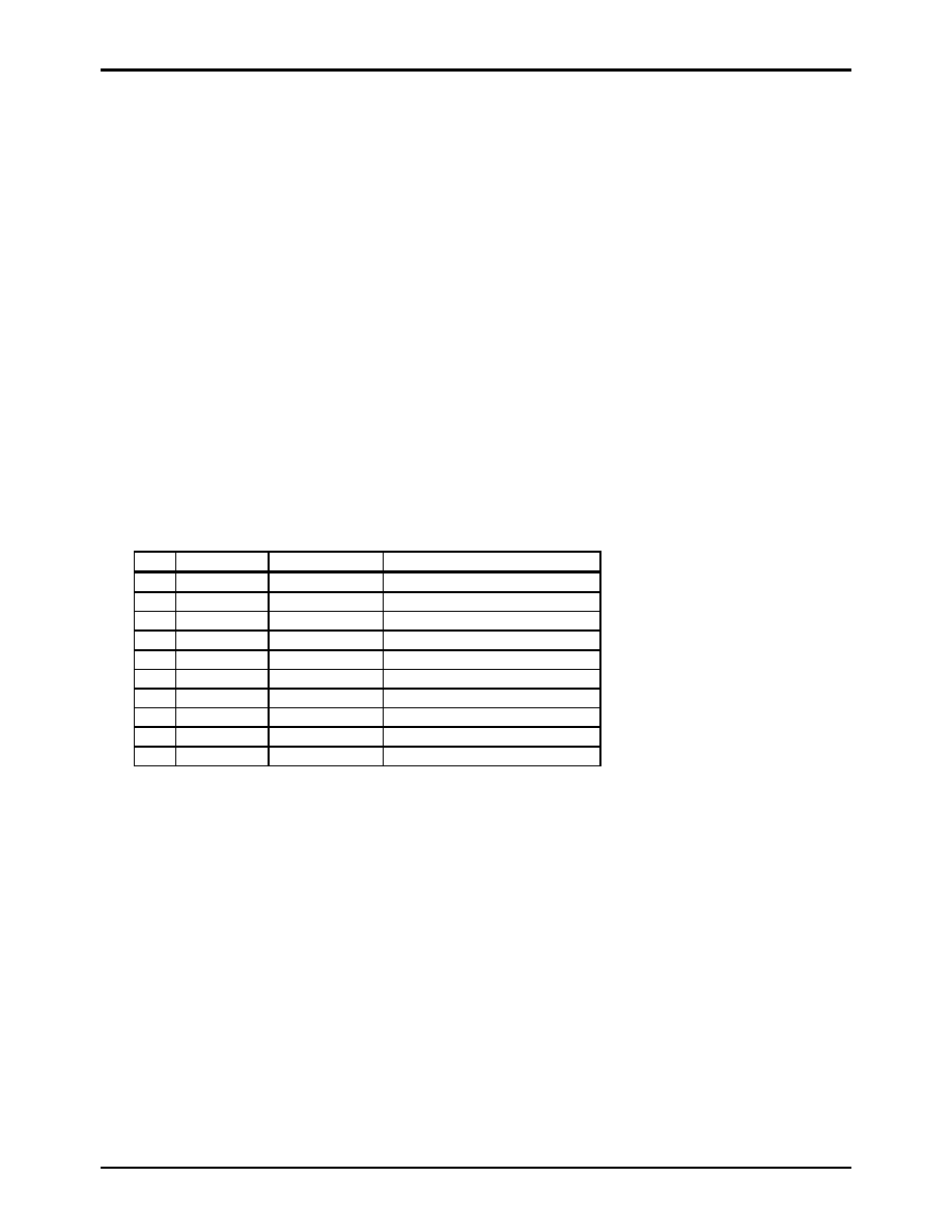
(13) Interrupts: 14 sources, 10 vectors
1) Three priority (low, high and highest) multiple interrupts are supported. During interrupt handling, an equal or
lower priority interrupt request is postponed.
2) If interrupt requests to two or more vector addresses occur at once, the higher priority interrupt takes precedence.
In the case of equal priority levels, the vector with the lowest address takes precedence.
No. Vector Selectable
Level
Interrupt
signal
1
00003H
X or L
INT0
2
0000BH
X or L
INT1
3
00013H
H or L
INT2/T0L
4
0001BH
H or L
INT3/Base timer
5
00023H
H or L
T0H
6
0002BH
H or L
T1L/T1H
7
00033H
H or L
SIO0
8
0003BH
H or L
SIO1
9
00043H
H or L
ADC/MIC
10
0004BH
H or L
Port 0
∑ Priority Level: X>H>L
∑ For equal priority levels, vector with lowest address takes precedence.
(14) Subroutine stack levels: 1024 levels max. Stack is located in RAM.
(15) Multiplication and division
- 16 bit
◊
8 bit (executed in 5 cycles)
- 24 bit
◊
16 bit (12 cycles)
- 16 bit ˜ 8 bit ( 8 cycles)
- 24 bit ˜ 16 bit (12 cycles)
(16) Oscillation circuits
- On-chip RC oscillation for system clock use.
- CF oscillation for system clock use. (Rf built in, Rd external)
- Crystal oscillation low speed system clock use. (Rf built in, Rd external)

LC87F72C8A
No.6712-4/24
(17) Standby function
- HALT mode
HALT mode is used to reduce power consumption. During the HALT mode, program execution is stopped but
peripheral circuits keep operating (some parts of serial transfer operation stop.)
1) Oscillation circuits are not stopped automatically.
2) Released by the system reset or interrupts.
-HOLD mode
HOLD mode is used to reduce power consumption. Program execution and peripheral circuits are stopped.
1) CF, RC and crystal oscillation circuits stop automatically.
2) Released by any of the following conditions.
1. Low level input to the reset pin
2. Specified level input to one of INT0, INT1, INT2
3. Port 0 interrupt
-X'tal HOLD made
X'tal HOLD mode is used to reduce power consumption. Program execution is stopped.
All peripheral circuits except the base timer are stopped.
1) CF and RC oscillation circuits stop automatically.
2) Crystal oscillator operation is kept in its state at HOLD mode inception.
3) Released by any of the following conditions
1. Low level input to the reset pin
2. Specified level input to one of INT0, INT1, INT2
3. Port 0 interrupt
4. Base-timer interrupt
(18) Package
- QIP100E
- SQFP100
(19) Development tools
- Evaluation chip: LC876096
- Emulator: EVA62S + ECB876500 (Evaluation chip board) + SUB877200 + POD100QFP or POD100SQFP (Type B)
(20) Same package and pin assignment as mask ROM version.
1) LC877200 series options can be set using flash ROM data. Thus the board used for mass production can
be used for debugging and evaluation without modifications.
2) If the program for the mask ROM version is used, the usable ROM/RAM capacity is the same as the mask
ROM version.
LC87F72C8A
No.6712-5/24
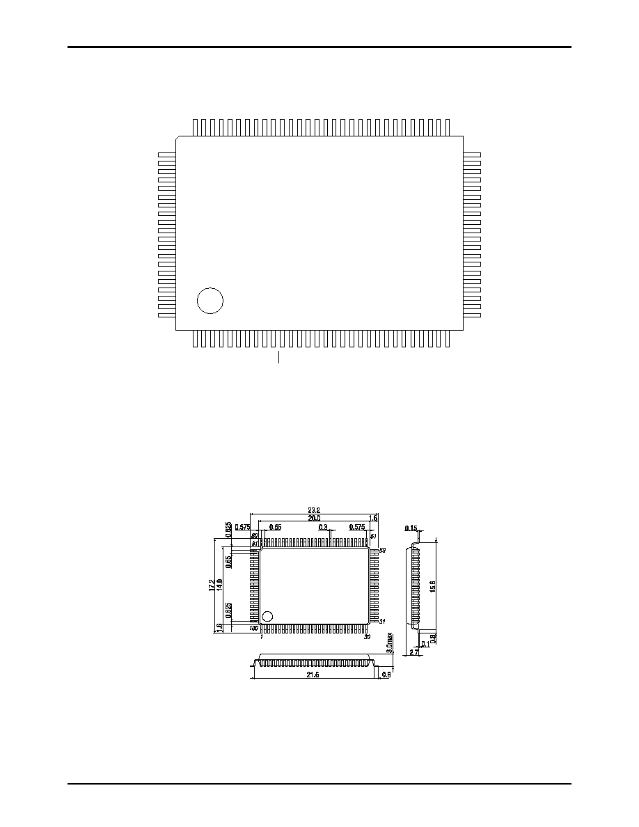
Pin Assignment
SANYO : QIP100-E
Package Dimension
(unit : mm)
3151
SANYO : QIP100-E
S20/PC4
S19/PC3
S18/PC2
S17/PC1
S16/PC0
S15/PB7
S14/PB6
S13/PB5
S12/PB4
S11/PB3
S10/PB2
S9/PB1
S8/PB0
S7/PA7
S6/PA6
S5/PA5
S4/PA4
S3/PA3
S2/PA2
S1PA1
V2/PL5
V1/PL4
COM0/PL0
COM1/PL1
COM2/PL2
COM3/PL3
P30
P31
VSS3
VDD3
P32
P33
P34
P35
P00
P01
P02
P03
P04
P05
P06
P07
P10
/
SO0
P11
/
SI0/
SB0
P12
/
SC
K
0
P13
/
SO1
P14
/
SI1/
SB1
P15
/
SCK1
P16
/
T1PW
M
L
P17
/
T1PW
M
H
/
B
U
Z
RE
S
XT1
/
A
N
10
XT2
/
A
N
11
VS
S1
CF
1
CF
2
VD
D1
P80
/
A
N
0
P81
/
A
N
1
P82
/
A
N
2
P83
/
A
N
3
P84
/
A
N
4
P85
/
A
N
5
P86
/
A
N
6
P87
/
A
N
7/
M
I
CIN
P
7
0
/
IN
T
0
/T
0L
C
P
/A
N
8
P
7
1
/
IN
T
1
/T
0H
C
P
/A
N
9
P72
/
INT2/
T
0IN
P73
/
INT3/
T
0IN
S0/
P
A0
V3
/
P
L
6
S47
/
PF
7
S46
/
PF
6
S45
/
PF
5
S44
/
PF
4
S43
/
PF
3
S42
/
PF
2
S41
/
PF
1
S40
/
PF
0
S39
/
PE7
S38
/
PE6
S37
/
PE5
S36
/
PE4
S35
/
PE3
S34
/
PE2
S33
/
PE1
S32
/
PE0
S31
/
PD7
S30
/
PD6
S29
/
PD5
S28
/
PD4
S27
/
PD3
S26
/
PD2
S25
/
PD1
S24
/
PD0
VS
S2
VD
D2
S23
/
PC7
S22
/
PC6
S21
/
PC5
1
2
3
4
5
6
7
8
9
10
11
12
13
14
15
16
17
18
19
20
21
22
23
24
25
26
27
28
29
30
80
79
78
77
76
75
74
73
72
71
70
69
68
67
66
65
64
63
62
61
60
59
58
57
56
55
54
53
52
51
50
49
48
47
46
45
44
43
42
41
40
39
38
37
36
35
34
33
32
31
81
82
83
84
85
86
87
88
89
90
91
92
93
94
95
96
97
98
99
100