CMOS LSI
Ordering number : EN4128B
83096HA (OT)/7062JN No. 4128-1/12
SANYO Electric Co.,Ltd. Semiconductor Bussiness Headquarters
TOKYO OFFICE Tokyo Bldg., 1-10, 1 Chome, Ueno, Taito-ku, TOKYO, 110 JAPAN
Digital Audio Interface Receiver
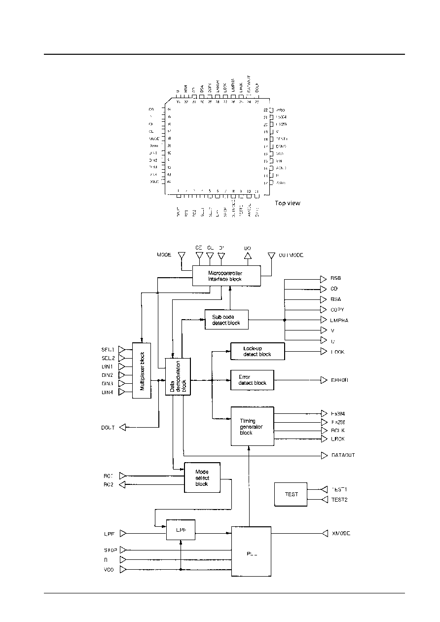
LC8900KQ
Overview
The LC8900KQ is a CMOS LSI circuit chip that can be
used to enable the EIAJ CP-1201 formatted data
transmission between digital audio equipment. It is used
by the receiving end and operates synchronously with
input signals. This chip demodulates input signals into
normally-formatted signals.
Features
∑ On-chip PLL circuit: enables the LSI operation to be
synchronous to the transmitted EIAJ format input
signals.
∑ Four input pins and one output pin: The output pin
enables the input data to be sent as they are.
∑ Two data output function modes: 20-bit data LSB first
mode and 16-bit data MSB first mode.
∑ Four output clocks: Bit clock, LRCK, 384Fs and 256Fs.
All these clocks are synchronized to the data.
∑ Various signal outputs: copy inhibit, emphasis on:off
control, user's bit, validity flag and sampling frequency.
∑ LPF time constant select mode: This function can be
used in the PLL lock-up state.
∑ Error detect signal output: If an input data error is
detected, this LSI circuit chip outputs the error signal.
In this case, the previous data will be output by the chip.
∑ Lock-up signal output: This signal is output when the
internal PLL (Phase Locked Loop) block of the LSI
circuit chip is locked.
∑ The chip has the pin to receive a signal for stopping the
PLL operation.
∑ Control and processing mode via microcontroller
interface: input pin select, copy information and
sampling frequency output.
∑ Each input pin has an internal amplifier circuit.
∑ Si gate, CMOS process technology and single 5V power
supply applicational and functional concept.
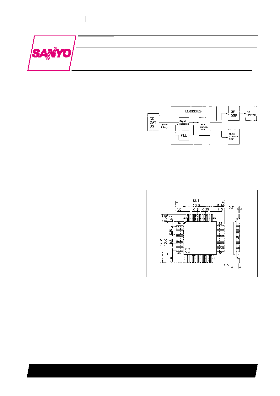
Applicational and Functional Concept
Package Dimensions
unit:mm
3148-QFP44MA
Preliminary
SANYO: QIP44MA
[LC8900KQ]
Pin Functions
No. 4128-3/12
LC8900KQ
Pin No.
Pin Name
I/O Type
Functional Description
1
DOUT
O
Input data output pin. However, its output is fixed at the low level if the DIN4 input pin is selected.
2
RC1
I
RC oscillation pin
3
RC2
O
RC oscillation pin
4
SEL1
I
Input pin select pin
5
SEL2
I
Input pin select pin
6
LPF
I
High level = LPF time constant select mode. low level = LPF time constant fixed mode. Fixed to high in most cases.
7
STOP
I
High = level:Forces the VCO operation to stop. Fixed to low in most cases.
I
Output data format select pin.
8
OUTMODE
High = 20-bit LSB first data format.
Low = 16-bit MSB first data format
9
TEST2
I
Test pin:Connected to the DGND in most cases.
10
XMODE
I
Input pin to start the PLL operation immediately after the LSI chip is powered on.
11
DV
DD
Digital power supply
12
AV
DD
Analog power supply
13
R
I
VCO oscillation bandwidth adjust pin
14
AGND
Analog ground
15
Vin
I
VCO self oscillation frequency setting pin
16
VCO
O
PLL LPF pin
17
DGND
Digital Ground
18
TEST1
I
Test pin:Connected to the DGND in most cases.
19
V
O
Validity flag output pin
20
FS256
O
256 Fs clock output pin
21
FS384
O
384 Fs clock output pin
22
DV
DD
Digital Power Supply
23
BCLK
O
Bit clock output pin
24
DATAOUT
O
Audio data output pin
25
LRCK
O
L/R clock output pin, Lch = high, Rch = low
26
EMPHA
O
Emphasis control (on/off) output pin:High = emphasis mode. Low = none-emphasis mode.
27
LOCK
O
PLL lock state output pin:High = PLL locked state. Low = PLL unlocked state.
28
ERROR
O
Input data error detect signal output:High = error detected.
29
COPY
O
Copy information output pin
30
BSA
O
Input data sampling frequency indication:High = 2 kHz.
31
CD
O
Input data sampling frequency indication:High = 44.1 kHz.
32
BSB
O
Input data sampling frequency indication:High = 48kHz.
33
U
O
User's bit output pin
34
DO
O
Microcontroller interface output pin
35
DI
I
Microcontroller interface input pin
36
CE
O
Microcontroller interface chip enable input pin
37
CL
O
Microcontroller interface clock input pin
38
MODE
I
Microcontroller interface control input:High = microcontroller interface active mode.
Low = microcontroller interface inactive mode.
39
DV
DD
Digital power supply
40
DIN1
I
Data input pin
41
DIN2
I
Data input pin
42
DIN3
I
Data input pin
43
DIN4
I
Data input pin
44
DGND
Digital ground
Specifications
Absolute Maximum Ratings
at Ta = 25∞C
Allowable Operating Range
at Ta = ≠30∞C to +75∞C
DC Characteristics
at Ta = ≠30 to +75∞C, V
DD
= 4.5 V to 5.5 V
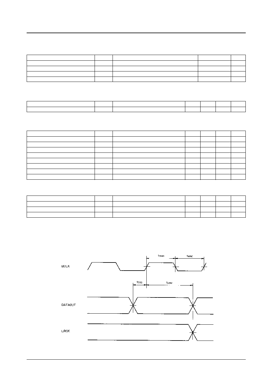
AC Characteristics
at Ta = ≠30 to 75∞C, V
DD
= 4.5 to 5.5 V
Note 1: All input pins except DIN1, DIN2, DIN3, DIN4 and XMODE.
Note 2: XMODE pin
Note 3: V
DD
=5.0V, Ta = 25
∞
C, input Fs=48 kHz.
Note 4: Before DIN1 to DIN4 input capacity is exceeded.
No. 4128-4/12
LC8900KQ
Parameter
Symbol
Conditions
Ratings
Unit
Maximum supply voltage
V
DD
max
Ta = 25∞C
≠0.3 to +7.0
V
Input/output voltage
V
I
∑ V
O
Ta = 25∞C
≠0.3 to V
DD
+0.3
V
Ambient operating temperature
Topr
≠30 to +75
∞C
Ambient storage temperature
Tstg
≠55 to +125
∞C
Parameter
Symbol
Conditions
min
typ
max
Unit
Supply voltage
V
DD
4.5
5.0
5.5
V
Parameter
Symbol
Conditions
min
typ
max
Unit
Input high level voltage
V
IH
*
1
2.2
V
DD
+ 0.3
V
Input low level voltage
V
IL
*
1
≠0.3
0.8
V
Input high level voltage
V
IH
*
2
0.8 V
DD
V
DD
+ 0.3
V
Input low level voltage
V
IL
*
2
≠0.3
0.2 V
DD
Output high level voltage
V
OH
I
OH
= ≠1 µA
V
DD
≠ 0.05
V
Output low level voltage
V
OL
I
OL
= 1 µA
V
SS
+ 0.05
V
Current drain
I
DD
*
3
11
12
mA
Input amplitude
V
IN
*
4
0.4
V
DD
+ 0.3
V
P
-
P
Parameter
Symbol
Conditions
min
typ
max
Unit
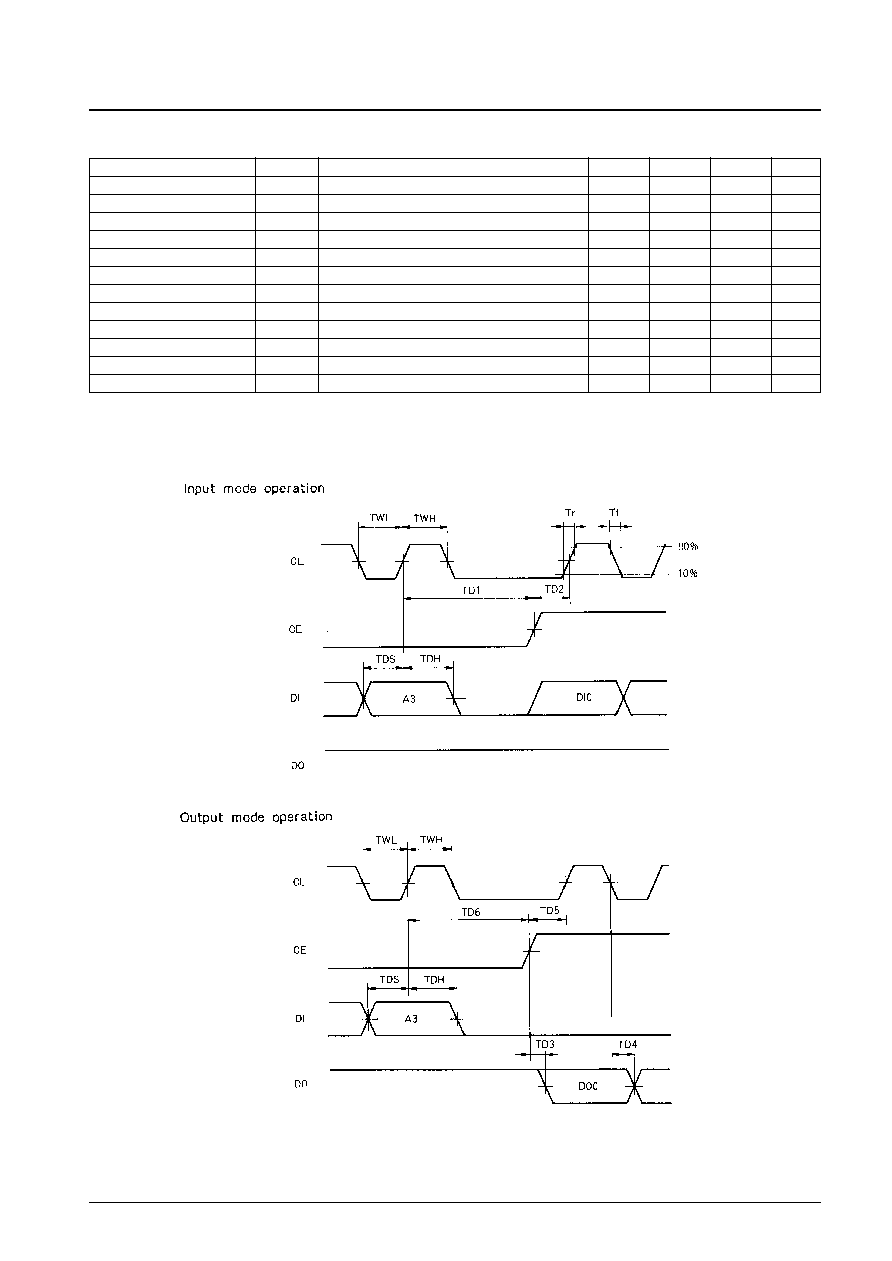
Output pulse width
t
WBO
Fs = 48kHz
160
ns
Output set-up time
t
DSO
80
ns
Output data hold time
t
DHO
80
ns