 | –≠–ª–µ–∫—Ç—Ä–æ–Ω–Ω—ã–π –∫–æ–º–ø–æ–Ω–µ–Ω—Ç: LC8901 | –°–∫–∞—á–∞—Ç—å:  PDF PDF  ZIP ZIP |
Ordering number : EN4079B
D3095HA (OT)/52593JN/7202JN No. 4079-1/15
Overview
The LC8901 and LC8901Q are LSIs for use in IEC958,
EIAJ CP-1201 format data transmission between digital
audio equipment. These LSIs are used on the receiving
side, and handle synchronization with the input signal and
demodulation of that signal to a normal format signal.
Features
∑ On-chip PLL circuit synchronizes with the transmitted
IEC958, EIAJ CP-1201 format signal.
∑ Provides 20-bit LSB first and 16-bit MSB first audio
data output functions.
∑ Microprocessor interface for mode settings and code
output
∑ System clock can be selected to be either 384fs or 512fs.
∑ Provides both a digital source mode and an analog
source mode.
∑ Fabricated in a Si-gate CMOS process.
∑ 5 V single-voltage power supply
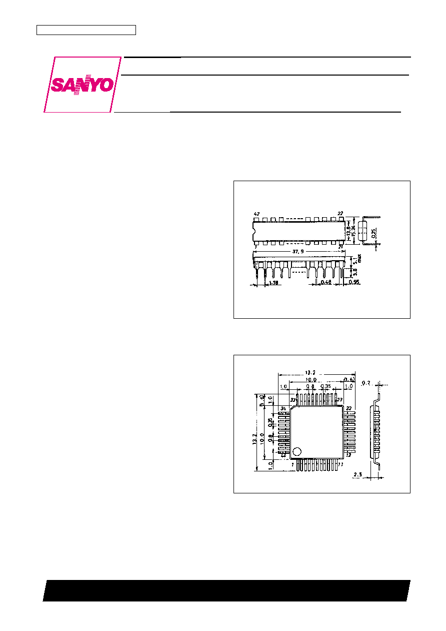
Package Dimensions
unit: mm
3025B-DIP42S
unit: mm
3148-QIP44M
SANYO: DIP42S
[LC8901]
SANYO: QIP44M
[LC8901Q]
LC8901, 8901Q
SANYO Electric Co.,Ltd. Semiconductor Bussiness Headquarters
TOKYO OFFICE Tokyo Bldg., 1-10, 1 Chome, Ueno, Taito-ku, TOKYO, 110-8534 JAPAN
Digital Audio Interface Receiver
CMOS LSI

Usage overview diagram
Assumes the use of both digital and analog source modes.
Digital source mode
Analog source mode
Pin Assignment
LC8901 (DIP42S)
LC8901Q (QIP44M)
No. 4079-2/15
LC8901, 8901Q
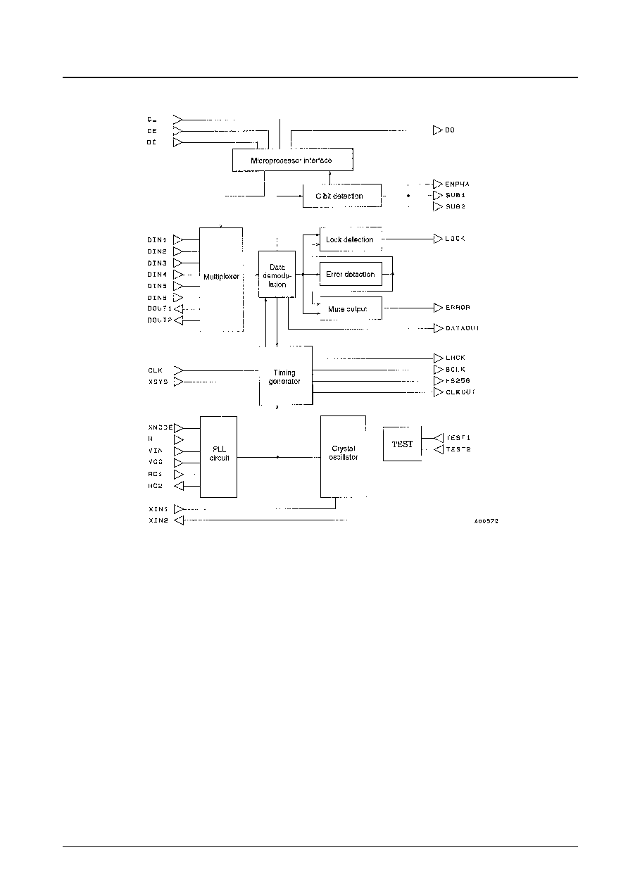
Block Diagram
No. 4079-3/15
LC8901, 8901Q
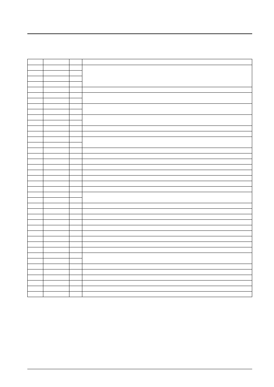
Pin Functions
LC8901 (DIP42S)
Note: The DIP42S package version has one fewer each of the digital system power supply and digital system ground pins than the QIP44M package version.
No. 4079-4/15
LC8901, 8901Q
Pin No.
Symbol
I/O
Pin function and circuit operation
1
DIN1
I
2
DIN2
I
Data input pins with built-in amplifiers
3
DIN3
I
4
DIN4
I
5
DGND
--
Digital system ground
6
DIN5
I
Data input pins without built-in amplifiers
7
DIN6
I
8
DOUT1
O
Input data through output
9
DOUT2
O
10
RC1
I
RC oscillator connection
11
RC2
O
12
LPF
I
High: LPF time constant switching mode, low: fixed mode. This pin is normally high.
13
STOP
I
High: VCO operation stopped, low: normal operation
14
TEST1
I
Test pins (These pins are normally low.)
15
TEST2
I
16
AV
DD
--
Analog system power supply
17
R
I
VCO oscillator band adjustment
18
AGND
--
Analog system ground
19
VIN
I
VCO free-running oscillator setup
20
VCO
O
PLL low-pass filter
21
DGND
--
Digital system ground
22
CLK
I
Clock mode switching. High: 512fs, low: 384fs
23
XSYS
I
Crystal mode setting. High: crystal mode
24
XIN1
I
Crystal oscillator connection
25
XIN2
O
26
DV
DD
--
Digital system power supply
27
LOCK
O
High: PLL locked, low: unlocked
28
ERROR
O
Error mute signal output
29
FS256
O
256fs clock output
30
CLKOUT
O
VCO oscillator and crystal oscillator clock output
31
EMPHA
O
High: emphasis present, low: no emphasis
32
BCLK
O
Bit clock output
33
DATAOUT
O
Audio data output
34
LRCK
O
Left/right clock output. High: left channel, low: right channel
35
SUB1
O
Sampling frequency output
36
SUB2
O
37
DO
O
Microprocessor interface output
38
DI
I
Microprocessor interface input
39
CE
I
Microprocessor interface chip enable input
40
CL
I
Microprocessor interface clock input
41
XMODE
I
Used to start system operation after power on.
42
DV
DD
--
Digital system power supply
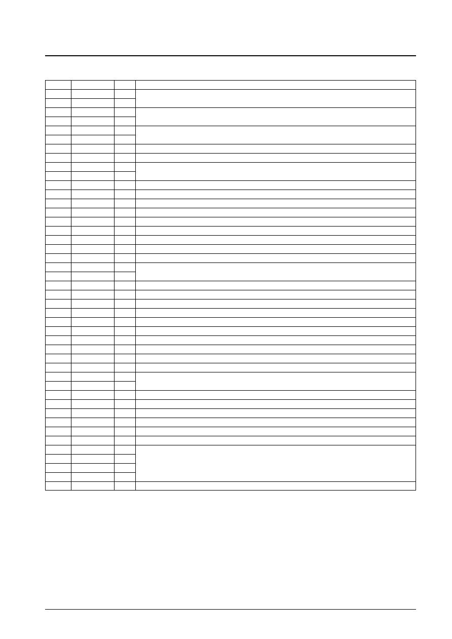
LC8901Q (QIP44M)
No. 4079-5/15
LC8901, 8901Q
Pin No.
Symbol
I/O
Pin function and circuit operation
1
DIN5
I
Data input pins without built-in amplifiers
2
DIN6
I
3
DOUT1
O
Input data through output
4
DOUT2
O
5
RC1
I
RC oscillator connection
6
RC2
O
7
LPF
I
High: LPF time constant switching mode, low: fixed mode. This pin is normally high.
8
STOP
I
High: VCO operation stopped, Low: normal operation
9
TEST1
I
Test pins (These pins are normally low.)
10
TEST2
I
11
DV
DD
--
Digital system power supply
12
AV
DD
--
Analog system power supply
13
R
I
VCO oscillator band adjustment
14
AGND
--
Analog system ground
15
VIN
I
VCO free-running oscillator setup
16
VCO
O
PLL low-pass filter
17
DGND
--
Digital system ground
18
CLK
I
Clock mode switching. High: 512fs, low: 384fs
19
XSYS
I
Crystal mode setting. High: crystal mode
20
XIN1
I
Crystal oscillator connection
21
XIN2
O
22
DV
DD
--
Digital system ground
23
LOCK
O
High: PLL locked, low: unlocked
24
ERROR
O
Error mute signal output
25
FS256
O
256fs clock output
26
CLKOUT
O
VCO oscillator and crystal oscillator clock output
27
EMPHA
O
High: emphasis present, low: no emphasis
28
DGND
--
Digital system ground
29
BCLK
O
Bit clock output
30
DATAOUT
O
Audio data output
31
LRCK
O
Left/right clock output. High: left channel, low: right channel
32
SUB1
O
Sampling frequency output
33
SUB2
O
34
DO
O
Microprocessor interface output
35
DI
I
Microprocessor interface input
36
CE
I
Microprocessor interface chip enable input
37
CL
I
Microprocessor interface clock input
38
XMODE
I
Used to start system operation after power on.
39
DV
DD
--
Digital system power supply
40
DIN1
I
41
DIN2
I
Data input pins with built-in amplifiers
42
DIN3
I
43
DIN4
I
44
DGND
--
Digital system ground