Ordering number : EN4542A
93094TH VL-0945, 0946/81793HK No. 4542-1/15
Overview
The LC8903 and LC8903Q are receiver LSIs for
applications in which data is transmitted between digital
audio equipment in the EIAJ format. These LSIs
synchronize with the input signal and demodulate that
signal to a regular format signal.
Features
∑ Built-in PLL circuit synchronizes with the input EIAJ
format signal.
∑ Microprocessor interface receives mode settings and
outputs fs codes, copy information, and category codes.
∑ Supports both 384 fs and 512 fs system clocks
(selectable) and provides 256 fs, 128 fs, BCLK and
LRCK clock outputs.
∑ Can operate in either digital source mode or analog
source mode.
∑ Validity flag output
∑ User bit CD subcode interface
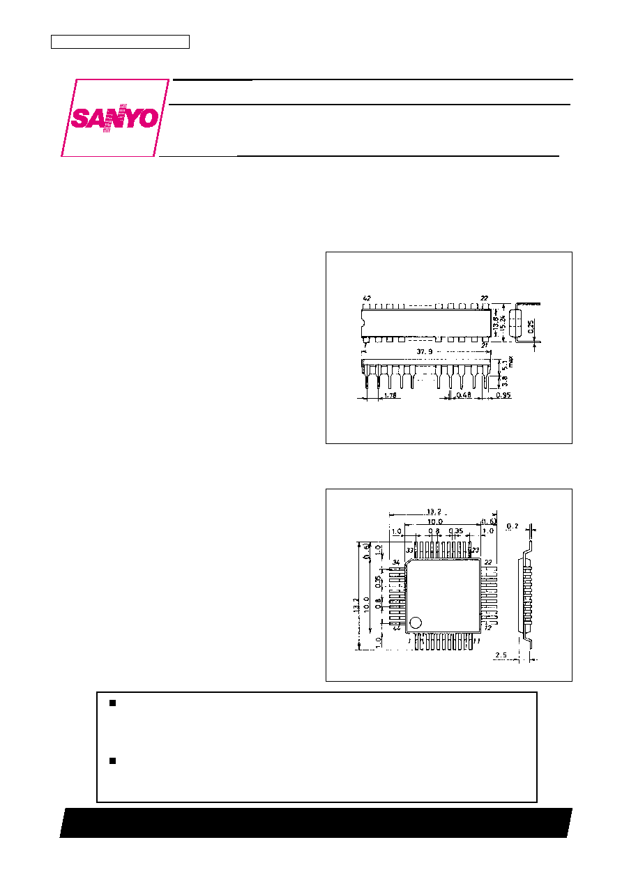
∑ DIP42S and QIP44M packages
∑ Silicon gate CMOS process, single 5 V power supply
Package Dimensions
unit: mm
3025B-DIP42S
unit: mm
3148-QFP44MA
SANYO: DIP42S
[LC8903]
SANYO: QIP44MA
[LC8903Q]
LC8903, 8903Q
SANYO Electric Co.,Ltd. Semiconductor Bussiness Headquarters
TOKYO OFFICE Tokyo Bldg., 1-10, 1 Chome, Ueno, Taito-ku, TOKYO, 110-8534 JAPAN
Digital Audio Interface Receiver
CMOS LSI
Any and all SANYO products described or contained herein do not have specifications that can handle
applications that require extremely high levels of reliability, such as life-support systems, aircraft's
control systems, or other applications whose failure can be reasonably expected to result in serious
physical and/or material damage. Consult with your SANYO representative nearest you before using
any SANYO products described or contained herein in such applications.
SANYO assumes no responsibility for equipment failures that result from using products at values that
exceed, even momentarily, rated values (such as maximum ratings, operating condition ranges, or other
parameters) listed in products specifications of any and all SANYO products described or contained
herein.

Application Usage Overview Diagram
When both digital source mode and analog source mode are used
Digital source mode:
EIAJ CP-1201 format data reception mode
Analog source mode: Analog data is received and converted to digital for signal processing.
This figure shows an example of a structure using the LC8903/Q. In analog source mode the only function of the
LC8903/Q is to provide control clocks.
Pin Assignments
Specifications
Absolute Maximum Ratings
at Ta = 25∞C
No. 4542-2/15
LC8903, 8903Q
Parameter
Symbol
Conditions
Ratings
Unit
Maximum supply voltage
V
DD
max
≠0.3 to +7.0
V
Maximum I/O voltages
V
I
∑V
O
max
≠0.3 to V
DD
+ 0.3
V
Operating temperature
Topr
≠30 to +75
∞C
Storage temperature
Tstg
≠55 to +125
∞C
Top view
Top view
Allowable Operating Ranges
DC Characteristics
at Ta = ≠30 to +75∞C, V
DD
= 4.5 to 5.5 V
Note: 1. Input pins other than DIN1, DIN2, DIN3, DIN4, RC1 and XMODE. TTL compatible.
2. XIN pin. CMOS compatible.
3. The XMODE and RC1 pins. CMOS Schmitt inputs.
4. The condition prior to the capacitors on the DIN1, DIN2, DIN3 and DIN4 input pins.
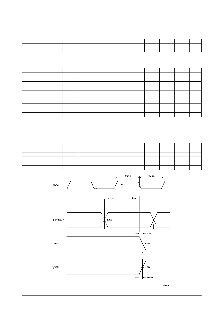
AC Characteristics
at Ta = ≠30 to +75∞C, V
DD
= 4.5 to 5.5 V
Note: 5. When validity is output from the V/DOUT2 pin.
No. 4542-3/15
LC8903, 8903Q
Parameter
Symbol
Conditions
min
typ
max
Unit
Supply voltage
V
DD
4.5
5.0
5.5
V
Operating temperature
Topg
≠30
+75
∞C
Parameter
Symbol
Conditions
min
typ
max
Unit
Output pulse width
t
WBO
fs = 48 kHz, with a 30 pF load capacitance
160
ns
Output setup time
t
DSO
80
ns
Output data hold time
t
DHO
80
ns
Output delay (high)
t
bdH
≠10
0
+10
ns
Output delay (low)
t
bdL
≠10
0
+10
ns
Parameter
Symbol
Conditions
min
typ
max
Unit
Input high level voltage
V
IH
1
*
1
2.2
V
DD
+ 0.3
V
Input low level voltage
V
IL
1
*
1
≠0.3
+0.8
V
Input high level voltage
V
IH
2
*
2
0.7 V
DD
V
DD
+ 0.3
V
Input low level voltage
V
IL
2
*
2
≠0.3
0.3 V
DD
V
Input high level voltage
V
IH
3
*
3
0.8 V
DD
V
DD
+ 0.3
V
Input low level voltage
V
IL
3
*
3
≠0.3
0.2 V
DD
V
Output high level voltage
V
OH
I
OH
= ≠1 µA
V
DD
≠ 0.05
V
Output low level voltage
V
OL
I
OL
= 1 µA
V
SS
+ 0.05
V
Current drain
I
DD
V
DD
= 5.0 V, Ta = 25∞C, input data fs = 48 kHz
10
20
30
mA
Input amplitude
V
PP
*
4
0.4
V
DD
+ 0.3
V
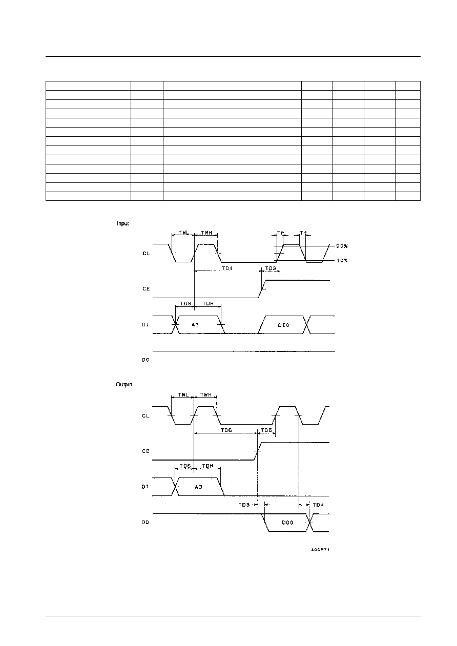
Microprocessor Interface Block AC Characteristics
at Ta = ≠30 to +75∞C, V
DD
= 4.5 to 5.5 V
No. 4542-4/15
LC8903, 8903Q
Parameter
Symbol
Conditions
min
typ
max
Unit
CL low level pulse width
TWL
100
ns
CL high level pulse width
TWH
100
ns
Data setup time
TDS
50
ns
Data hold time
TDH
50
ns
CL rise time
Tr
CL, CE, DI
30
ns
CL fall time
Tf
CL, CE, DI
30
ns
CE delay time
TD1
1.0
µs
CL delay time
TD2
50
ns
Data delay time
TD3
With a 30 pF load capacitance
25
ns
CL, data delay time
TD4
With a 30 pF load capacitance
50
ns
CL delay time
TD5
100
ns
CL, CE delay time
TD6
1.0
µs

CD Subcode Interface AC Characteristics
at Ta = ≠30 to +75∞C, V
DD
= 4.5 to 5.5 V
Note: Assumes that the load capacitance on each output pin is 30 pF.
No. 4542-5/15
LC8903, 8903Q
Parameter
Symbol
Conditions
min
typ
max
Unit
SBSY block frequency
tB
12.0
13.3
14.7
ms
SBSY pulse width
tBW
*
6
110
µs
SFSY frame frequency
tF
*
7
90
136
165
µs
SFSY high level pulse width
tFHW
4
µs
SFSY low level pulse width
tFLW
1.5
µs
SBCK high level pulse width
tCHW
*
8
2.0
4.0
5.0
µs
SBCK low level pulse width
tCLW
*
8
2.0
4.0
5.0
µs
SBCK rise time
trC
30
ns
SBCK fall time
tfC
30
ns
SBCK delay time
tCD
*
8
10
20
30
µs
P data access
tPAC
3
10
µs
Data hold time
tHD
0
µs