Ordering number : EN
*
5014B
73096HA (OT) No. 5014-1/20
Overview
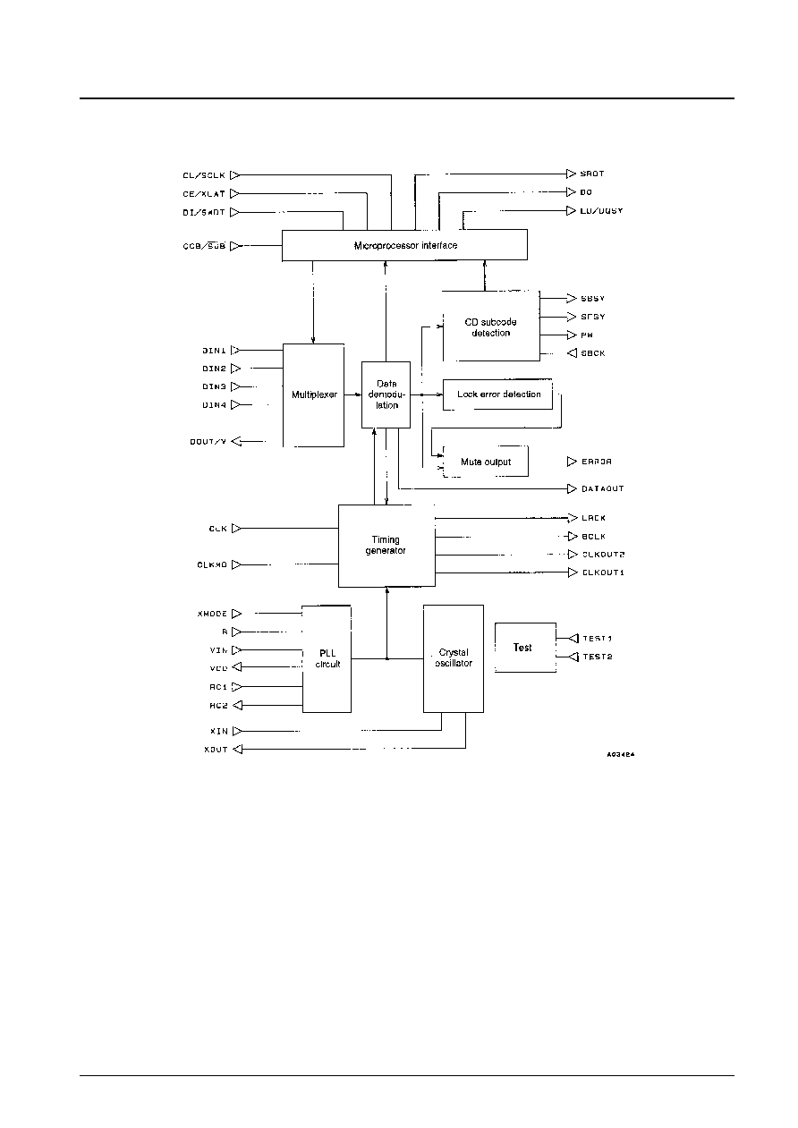
The LC8904Q demodulates data transmitted between
digital audio equipment in the EIAJ format (CP-1201) to a
normal format signal synchronized with the receiving side
input signal.
Features
∑ Synchronizes with the transmitted EIAJ format signal
using a built-in PLL circuit.
∑ Modes are set up and codes are output according to
commands sent over a microprocessor interface.
-- Input pin and output data format setup
-- Selection of digital source mode or analog source
mode
-- 32-bit channel status output (consumer product
mode 0)
-- 80-bit subcode Q data output (CRC check included)
∑ Either a 384fs or a 512fs clock can be selected as the
system clock.
∑ Provides 256fs, 128fs, BCLK, and LRCK clock outputs.
∑ Implements a CD subcode interface (CP-2401) using
user bits.
∑ Fabricated in a CMOS single-voltage power supply
process
∑ Package: QFP-48E
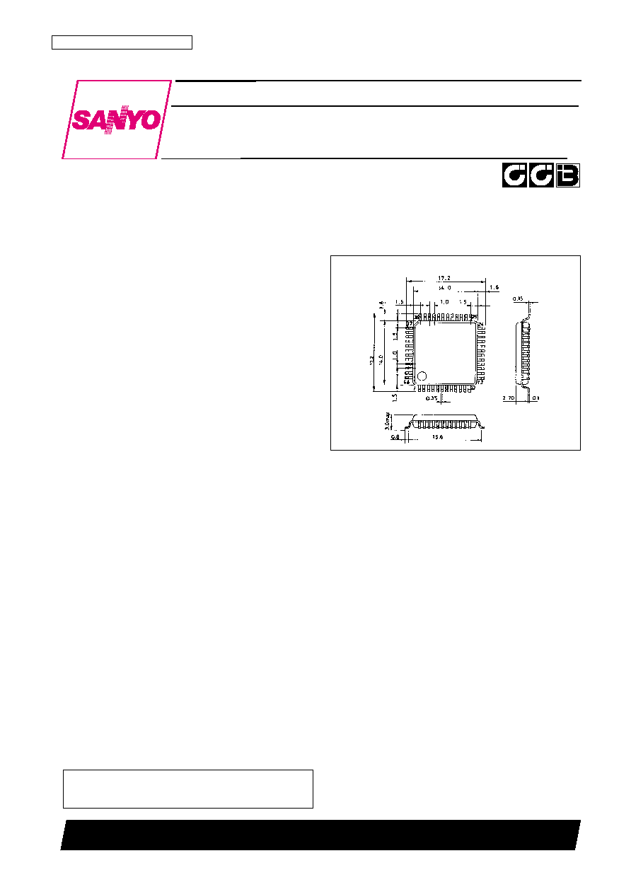
Package Dimensions
unit: mm
3156-QFP48E
Preliminary
SANYO: QIP48E
[LC8904Q]
LC8904Q
SANYO Electric Co.,Ltd. Semiconductor Bussiness Headquarters
TOKYO OFFICE Tokyo Bldg., 1-10, 1 Chome, Ueno, Taito-ku, TOKYO, 110-0005 JAPAN
Digital Audio Interface Receiver
CMOS LSI
∑ CCB is a trademark of SANYO ELECTRIC CO., LTD.
∑ CCB is SANYO's original bus format and all the bus
addresses are controlled by SANYO.
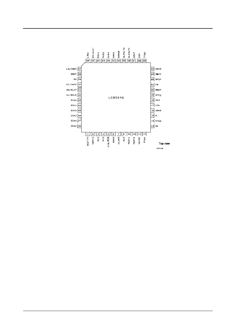
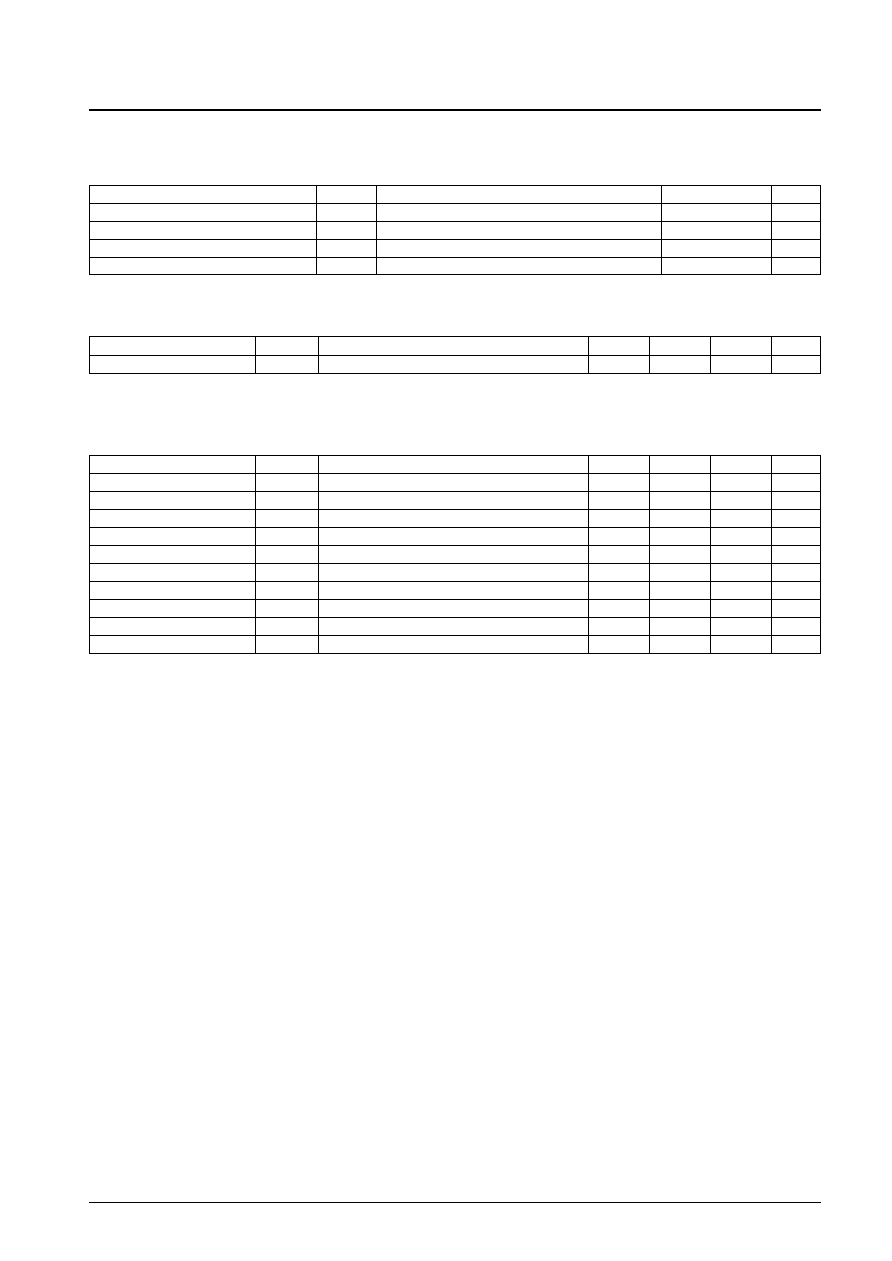
Pin Functions
No. 5014-4/20
LC8904Q
No.
Symbol
I/O
Function
1
DOUT/V
O
EIAJ data and validity flag output
2
EMPHA
O
Emphasis monitor output (High: emphasis applied)
3
RC1
I
CR oscillator input
4
RC2
O
CR oscillator output
5
CCB/SUB
I
Microprocessor interface selection input (High: CCB, low: SUB)
6
DGND
Digital system ground
7
CLKMD
I
Clock output switching (High: 256fs, low: 128fs)
8
CLK
I
Clock switching input (High: 512fs, low: 384fs)
9
TEST1
I
Test pin (Must be tied low during normal operation.)
10
TEST2
I
Test pin (Must be tied low during normal operation.)
11
XMODE
I
Reset input
12
DV
DD
Digital system power supply
13
NC
No connection
14
AV
DD
Analog system power supply
15
R
I
VCO oscillator band adjustment input
16
AGND
Analog system ground
17
VIN
I
VCO free-running frequency setting input
18
VCO
O
PLL low-pass filter connection
19
DV
DD
Digital system power supply
20
SBSY
O
CD subcode interface: block sync output
21
PW
O
CD subcode interface: data output
22
SFSY
O
CD subcode interface: frame sync output
23
SBCK
I
CD subcode interface: data read shift clock input
24
DGND
Digital system ground
25
DV
DD
Digital system power supply
26
XIN
I
Crystal oscillator input
27
XOUT
O
Crystal oscillator output
28
CLKOUT1
O
VCO and crystal oscillator clock output
29
CLKOUT2
O
256fs or 128fs clock output (selected by CLKMD)
30
ERROR
O
Error mute output
31
DGND
Digital system ground
32
SUB1
O
Sampling frequency monitor output
33
SUB2
O
Sampling frequency monitor output
34
BCLK
O
Bit clock output
35
DATAOUT
O
Audio data output
36
LRCK
O
L/R clock output (High: left channel, low: right channel)
37
LD/DQSY
O
Microprocessor interface: subcode Q data sync output
38
SRDT
O
Microprocessor interface: data output when CCB/SUB is low (3-state output)
39
DO
O
Microprocessor interface: data output when CCB/SUB is high (High-level open drain output)
40
DI/SWDT
I
Microprocessor interface: data input
41
CE/XLAT
I
Microprocessor interface: chip enable/latch input
42
CL/SCLK
I
Microprocessor interface: clock input
43
DV
DD
Digital system power supply
44
DIN1
I
Data input with built-in amplifier
45
DIN2
I
Data input with built-in amplifier
46
DIN3
I
Data input with built-in amplifier
47
DIN4
I
Data input with built-in amplifier
48
DGND
Digital system ground
Specifications
Absolute Maximum Ratings
at Ta = 25∞C
Allowable Operating Ranges
Electrical Characteristics
DC Characteristics
at Ta = ≠30 to +75∞C, V
DD
= 4.5 to 5.5 V
Note: 1. Input pins other than DIN1, DIN2, DIN3, DIN4, RC1, and XMODE. TTL compatible.
2. The XIN pin. CMOS compatible.
3. The XMODE and RC1 pins. CMOS Schmitt compatible.
4. V
DD
= 5.0 V, Ta = 25∞C, and input data with an fs of 48 kHz.
5. Conditions prior to the capacitances of the DIN1, DIN2, DIN3, and DIN4 pins.
No. 5014-5/20
LC8904Q
Parameter
Symbol
Conditions
Ratings
Unit
Maximum supply voltage
V
DD
max
≠0.3 to +7.0
V
Input and output voltage
V
I
∑ V
O
≠0.3 to V
DD
+ 0.3
V
Operating temperature
Topr
≠30 to +75
∞C
Storage temperature
Tstg
≠55 to +125
∞C
Parameter
Symbol
Conditions
min
typ
max
Unit
Supply voltage
V
DD
4.5
5.0
5.5
V
Parameter
Symbol
Conditions
min
typ
max
Unit
Input high-level voltage
V
IH
1
*
1
2.2
V
DD
+ 0.3
V
Input low-level voltage
V
IL
1
*
1
≠0.3
+0.8
V
Input high-level voltage
V
IH
2
*
2
0.7 V
DD
V
DD
+ 0.3
V
Input low-level voltage
V
IL
2
*
2
≠0.3
0.3 V
DD
V
Input high-level voltage
V
IH
3
*
3
0.8 V
DD
V
DD
+ 0.3
V
Input low-level voltage
V
IL
3
*
3
≠0.3
0.2 V
DD
V
Output high-level voltage
V
OH
I
OH
= ≠1 µA
V
DD
≠ 0.05
V
Output low-level voltage
V
OL
I
OL
= 1 µA
V
SS
+ 0.05
V
Current drain
I
DD
*
4
30
45
mA
Input amplitude
V
PP
*
5
0.4
V
DD
+ 0.3
V