 | –≠–ª–µ–∫—Ç—Ä–æ–Ω–Ω—ã–π –∫–æ–º–ø–æ–Ω–µ–Ω—Ç: LC89066M | –°–∫–∞—á–∞—Ç—å:  PDF PDF  ZIP ZIP |
6-Bit Video A/D Converters
Overview
The LC89066 and LC89066M are high-speed analog-to-digital
converters. They are of flash type, operate from single 5V
supply, and feature a 15 Mega-samples per second conversion
rate and low power dissipation.
Features
.
Conversion rate: 15 MSPS
.
Low power dissipation: 120 mW
.
Linearity error within
±
0.8 LSB (max)
.
TTL-compatible inputs
.
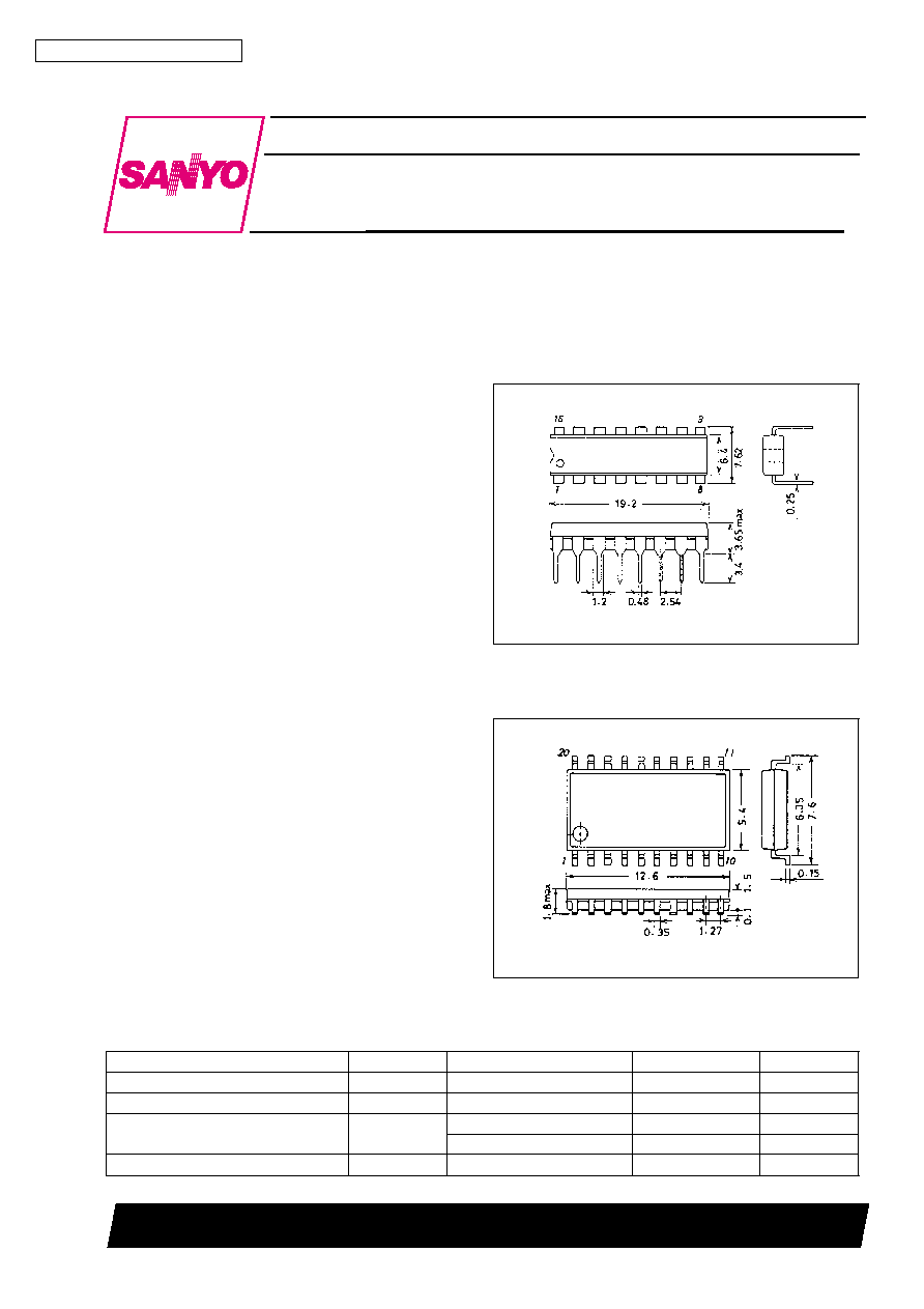
LC89066: DIP-16
LC89066M: MFP-20
Package Dimensions
unit : mm
3006B-DIP16
[LC89066]
SANYO : DIP16
unit : mm
3036B-MFP20
[LC89066M]
SANYO : MFP20
Specifications
Absolute Maximum Ratings
at Ta = 25 ∞C, V
SS
= 0 V
Parameter
Symbol
Conditions
Ratings
Unit
Maximum supply voltage
V
DD
max
≠0.3 to +7.0
V
Input voltage
V
IN
≠0.3 to V
DD
+0.3
V
Operating temperature
Topr
LC89066
≠30 to +75
∞C
LC89066M
≠30 to +65
∞C
Storage temperature
Tstg
≠40 to +125
∞C
Ordering number: EN3086B
CMOS LSI
LC89066, 89066M
SANYO Electric Co.,Ltd. Semiconductor Bussiness Headquarters
TOKYO OFFICE Tokyo Bldg., 1-10, 1 Chome, Ueno, Taito-ku, TOKYO, 110 JAPAN
13097HA(II)/8099TA,TS(US) No.3086-1/4
Recommended Operating Conditions
Parameter
Symbol
Conditions
min
typ
max
Unit
Supply voltage
V
DD
4.75
5.0
5.25
V
Reference voltage (high)
V
RH
V
DD
V
Reference voltage (low)
V
RL
0
V
Input high-level voltage
V
IH
2.2
V
DD
+0.3
V
Input low-level voltage
V
IL
≠0.3
+0.8
V
Analog input voltage
V
ANI
V
RL
V
RH
V
Clock high period
T
WH
30
ns
Clock low period
T
WL
30
ns
Electrical Characteristics
at Ta = 25 ∞C, V
DD
= 5.0 V, V
RH
= 5.0 V, V
RL
= 3.0 V
Parameter
Symbol
Conditions
min
typ
max
Unit
Resolution
RES
6
bit
Maximum sampling frequency
Fs max
15
MSPS
Power dissipation
Pd
Fs = 15 MSPS
120
200
mW
Linearity error
I.L.
DC accuracy
±
0.8
LSB
Differential linearity error
D.L.
DC accuracy
±
0.5
LSB
String resistance
Rst
400
600
800
Analog input capacitance
C
AIN
50
pF
Analog input resistance
R
AIN
10
M
Output delay time
TdL
20
45
ns
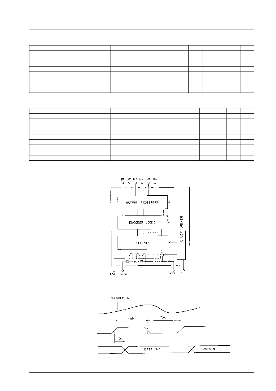
Equivalent Circuit Block Diagram
Timing Chart
Analog input
Clock input
Digital signal output
LC89066, 89066M
No.3086-2/4
Pin Functions
.
LC89066
Pin No.
Symbol
Description
1
D6
Digital output data (least significant bit)
2
D5
Digital output data
3
D4
4
D3
5
D2
6
D1
Digital output data (most significant bit)
7
CLK
Clock input
8
GND
Ground (analog)
9
V
DD
Power supply (analog)
10
V
DD
11
V
RH
Reference voltage input (high)
12
ANI
Analog voltage input
13
V
RL
Reference voltage input (low)
14
V
DD
Power supply (digital)
15
V
DD
16
GND
Ground (digital)
.
LC89066M
Pin No.
Symbol
Description
1
D6
Digital output data (least significant bit)
2
D5
Digital output data
3
N.C.
No connection
4
D4
Digital output data
5
D3
6
D2
7
D1
Digital output data (most significant bit)
8
N.C.
No connection
9
CLK
Clock input
10
GND
Ground (analog)
11
V
DD
Power supply (analog)
12
V
DD
13
N.C.
No connection
14
V
RH
Reference voltage input (high)
15
ANI
Analog voltage input
16
V
RL
Reference voltage input (low)
17
V
DD
Power supply (digital)
18
N.C.
No connection
19
V
DD
Power supply (digital)
20
GND
Ground (digital)
Functional Description
Signal on the analog signal input pin ANI is input into the comparators on the rising edge of the CLK input signal. This signal is
compared with the voltage divided by resistors and digitized. This digitized signal is coded by the encoder logic and output on the
next rising edge of the CLK input signal. The conversion range depends on the converter high and low reference voltage V
RH
and
V
RL
. When zero transient voltage is set to 3.000 V by V
RL
voltage and full scale transient voltage to 4.984 V by V
RH
voltage, the
output data is linearly related to the input voltage as shown in the table below.
Input voltage (V)
Output data
0
to 3.000
000000
1
3.000 to 3.032
000001
2
3.032 to 3.064
000010
3
3.064 to 3.096.
000011
.
.
.
.
.
.
.
.
.
.
.
.
61
4.920 to 4.952
111101
62
4.952 to 4.984
111110
63
4.984 to
111111
LC89066, 89066M
No.3086-3/4

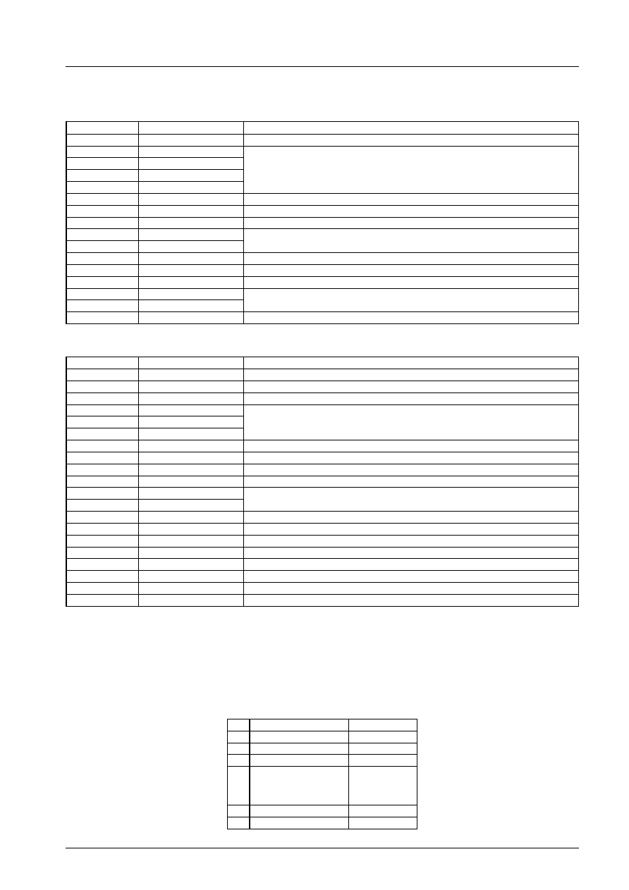
Sample Application Circuits
The following diagrams show typical application circuits for the LC89066 and LC89066M. The high reference voltage is
connected to the positive supply line, and the low reference voltage generated by a voltage divider and emitter follower. The
analog signal is input with a low impedance.
No products described or contained herein are intended for use in surgical implants, life-support systems, aerospace equipment,
nuclear power control systems, vehicles, disaster/crime-prevention equipment and the like, the failure of which may directly or
indirectly cause injury, death or property loss.
Anyone purchasing any products described or contained herein for an above-mentioned use shall:
1
Accept full responsibility and indemnify and defend SANYO ELECTRIC CO., LTD., its affiliates, subsidiaries and distributors
and all their officers and employees, jointly and severally, against any and all claims and litigation and all damages, cost and
expenses associated with such use:
2
Not impose any responsibility for any fault or negligence which may be cited in any such claim or litigation on SANYO
ELECTRIC CO., LTD., its affiliates, subsidiaries and distributors or any of their officers and employees jointly or severally.
Information (including circuit diagrams and circuit parameters) herein is for example only; it is not guaranteed for volume
production. SANYO believes information herein is accurate and reliable, but no guarantees are made or implied regarding its use
or any infringements of intellectual property rights or other rights of third parties.
This catalog provides information as of January, 1997. Specifications and information herein are subject to change without notice.
Digital
signal
output
Power supply
Oscillator
Analog
input
Power supply
Digital
signal
output
Oscillator
Analog
input
LC89066, 89066M
No.3086-4/4