 | –≠–ª–µ–∫—Ç—Ä–æ–Ω–Ω—ã–π –∫–æ–º–ø–æ–Ω–µ–Ω—Ç: LC89080 | –°–∫–∞—á–∞—Ç—å:  PDF PDF  ZIP ZIP |
Ordering number : EN
*
4030A
D3095HA (OT)/5272TS No. 4030-1/8
Overview
The LC89080 and LC89080Q are high-speed current-
output D/A converters. They feature 8-bit resolution,
provide 3 channels on a single chip, and can be used in
demodulators for high-speed signals such as video signals.
Features
∑ Resolution: 8 bits
∑ D/A converters: Three current-output D/A converter
channels on a single chip
∑ Maximum conversion speed: 30 MSPS
∑ Error: ±1.0 LSB (maximum)
∑ Power supply: +5 V single-voltage power supply
∑ Power dissipation: 330 mW
∑ Inputs: TTL compatible
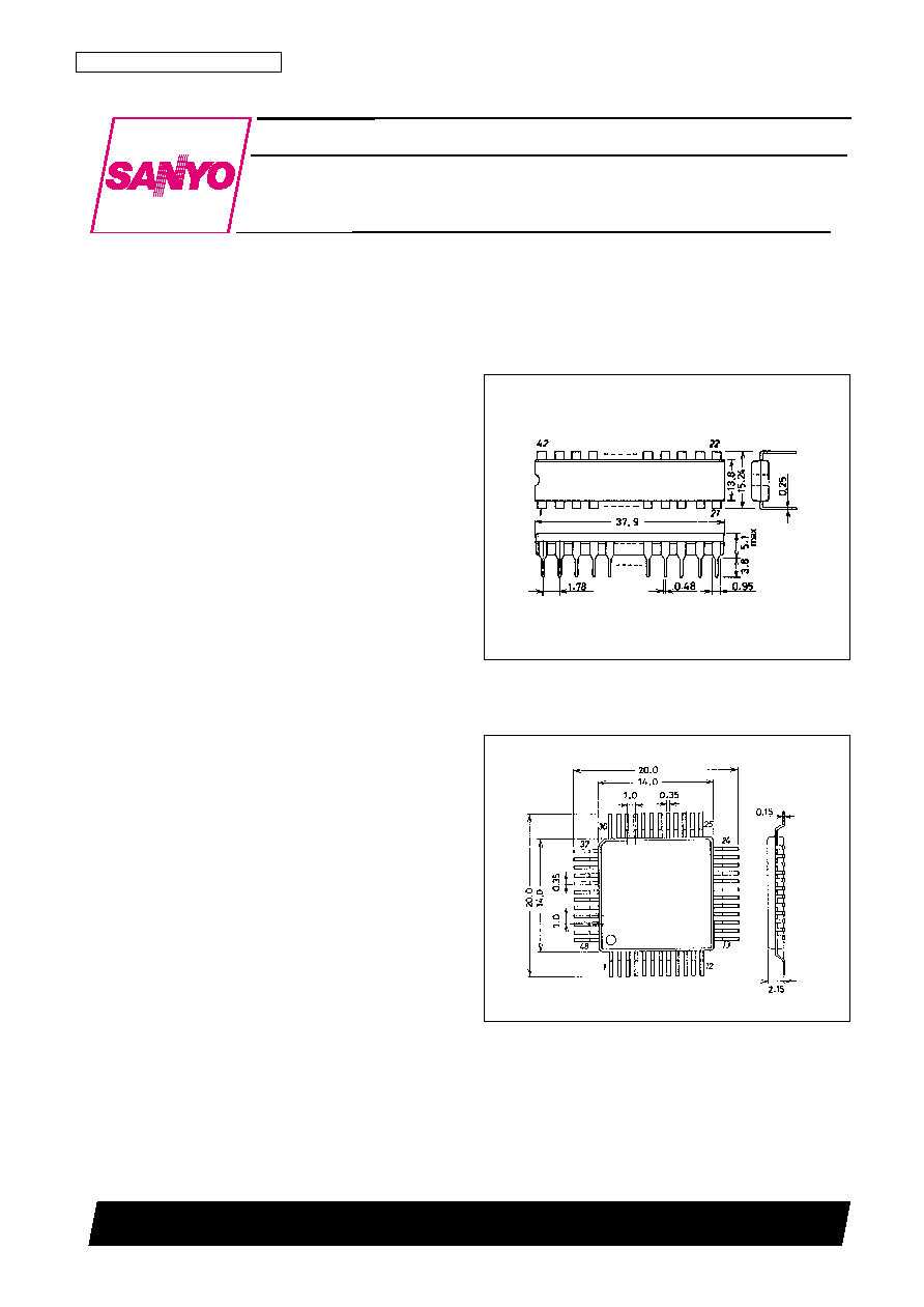
Package Dimensions
unit: mm
3025B-DIP42S
unit: mm
3052A-QFP48A
Preliminary
SANYO: DIP42S
[LC89080]
SANYO: QFP48A
[LC89080Q]
LC89080, 89080Q
SANYO Electric Co.,Ltd. Semiconductor Bussiness Headquarters
TOKYO OFFICE Tokyo Bldg., 1-10, 1 Chome, Ueno, Taito-ku, TOKYO, 110-8534 JAPAN
Video Signal 3-Channel 8-Bit D/A Converter
CMOS LSI
Specifications
Absolute Maximum Ratings
at Ta = 25∞C, V
SS
= 0 V
Allowable Operating Ranges
Electrical Characteristics
at Ta = 25∞C, V
DD
= 5.0 V, V
REF
IN = 1.0 V, R
REF
= 300
, R
O
= 75
No. 4030-2/8
LC89080, 89080Q
Parameter
Symbol
Conditions
Ratings
Unit
Maximum supply voltage
V
DD
max
≠0.3 to +7.0
V
Input voltage
V
IN
≠0.3 to V
DD
+ 0.3
V
Operating temperature
Topr
≠30 to +75
∞C
Storage temperature
Tstg
≠40 to +125
∞C
Parameter
Symbol
Conditions
min
typ
max
Unit
Supply voltage
V
DD
4.5
5.0
5.5
V
Reference voltage input
V
REF
IN
1.0
2.0
V
Output resistance
R
O
75
Input high-level voltage
V
IH
2.2
V
DD
+ 0.3
V
Input low-level voltage
V
IL
≠0.3
+0.8
V
Phase compensation capacitance
Ccomp
1
µF
Parameter
Symbol
Conditions
min
typ
max
Unit
Resolution
RES
8
Bits
Maximum conversion speed
Fs max
30
MSPS
Power dissipation
Pd
Fs = 30 MSPS
330
400
mW
Zero-scale output voltage
Vzero
For each channel
≠15
0
+15
mV
Full-scale output voltage
Vfull
For each channel
0.92
1.00
1.08
V
Full-scale voltage ratio
FSR
0
4
8
%
Linearity error
I.L.
DC precision
±1.0
LSB
Differential linearity error
D.L.
DC precision
±0.5
LSB
Reference voltage output
V
REF
OUT
0.99
1.00
1.01
V
Pin Assignment LC89080 (DIP42S)
No. 4030-3/8
LC89080, 89080Q
Pin No.
Symbol
Description
1
DV
DD
Digital system power supply (+5 V)
2
DA1
Channel A digital input (MSB)
3 to 8
DA2 to DA7
Channel A digital input
9
DA8
Channel A digital input (LSB)
10
DB1
Channel B digital input (MSB)
11 to 16
DB2 to DB7
Channel B digital input
17
DB8
Channel B digital input (LSB)
18
DC1
Channel C digital input (MSB)
19 to 24
DC2 to DC7
Channel C digital input
25
DC8
Channel C digital input (LSB)
26
CLK
Clock input
27
DV
DD
Digital system power supply (+5 V)
28
DGND
Digital system ground (0 V)
29
ICOB
Channel C negative output. Connect to A.GND through an output resistor R
O
(usually 75
).
30
ICO
Channel C positive output. Connect to A.GND through an output resistor R
O
(usually 75
).
31
AV
DD
Analog system power supply (+5 V)
32
IBOB
Channel B negative output. Connect to A.GND through an output resistor R
O
(usually 75
).
33
IBO
Channel B positive output. Connect to A.GND through an output resistor R
O
(usually 75
).
34
AGND
Analog system ground (0 V)
35
IAOB
Channel A negative output. Connect to A.GND through an output resistor R
O
(usually 75
).
36
IAO
Channel A positive output. Connect to A.GND through an output resistor R
O
(usually 75
).
37
AV
DD
Analog system power supply (+5 V)
38
COMP
Phase compensation capacitor. Connect a 1 µF capacitor between this pin and ground.
39
I
REF
Reference current output. Connect a resistor that is 4 times the output resistance R
O
to this pin.
40
V
REF
IN
Reference voltage input. This input pin sets the analog output dynamic range.
41
V
REF
OUT
Reference voltage output. The output voltage is set to 0.2 times V
DD
by a resistor divider.
When V
DD
is 5.0 V, a 1.0 V reference voltage can be acquired from pin 40.
42
DGND
Digital system ground (0 V)

Pin Assignment LC89080Q (QFP48A)
No. 4030-4/8
LC89080, 89080Q
Pin No.
Symbol
Description
1 to 3
DA5 to 7
Channel A digital input
4
DA8
Channel A digital input (LSB)
5
DB1
Channel B digital input (MSB)
6
NC
Unused (no connection)
7 to 12
DB2 to DB7
Channel B digital input
13
DB8
Channel B digital input (LSB)
14
DC1
Channel C digital input (MSB)
15 to 18
DC2 to DC5
Channel C digital input
19
DV
DD
Digital system power supply (+5 V)
20
DC6
Channel C digital input
21
DC7
Channel C digital input
22
DC8
Channel C digital input (LSB)
23
CLK
Clock input
24
NC
Unused (no connection)
25
DV
DD
Digital system power supply (+5 V)
26
DGND
Digital system ground (0 V)
27
ICOB
Channel C negative output. Connect to A.GND through an output resistor R
O
(usually 75
).
28
ICO
Channel C positive output. Connect to A.GND through an output resistor R
O
(usually 75
).
29
AV
DD
Analog system power supply (+5 V)
30
AV
DD
Analog system power supply (+5 V)
31
IBOB
Channel B negative output. Connect to A.GND through an output resistor R
O
(usually 75
).
32
IBO
Channel B positive output. Connect to A.GND through an output resistor R
O
(usually 75
).
33
AGND
Analog system ground (0 V)
34
IAOB
Channel A negative output. Connect to A.GND through an output resistor R
O
(usually 75
).
35
IAO
Channel A positive output. Connect to A.GND through an output resistor R
O
(usually 75
).
36
AV
DD
Analog system power supply (+5 V)
37
COMP
Phase compensation capacitor. Connect a 1 µF capacitor between this pin and ground.
38
NC
Unused (no connection)
39
I
REF
Reference current output. Connect a resistor that is 4 times the output resistance R
O
to this pin.
40
V
REF
IN
Reference voltage input. This input pin sets the analog output dynamic range.
41
V
REF
OUT
Reference voltage output. The output voltage is set to 0.2 times V
DD
by a resistor divider.
When V
DD
is 5.0 V, a 1.0 V reference voltage can be acquired from pin 40.
42
DGND
Digital system ground (0 V)
43
DV
DD
Digital system power supply (+5 V)
44
DV
DD
Digital system power supply (+5 V)
45
DA1
Channel A digital input (MSB)
46 to 48
DA2 to DA4
Channel A digital input
LC89080 Operation
The LC89080 and LC89080Q include three current-matrix D/A converters on chip. These D/A converters each have 63
basic current cells (with current weight I) and two weighted current cells (I/2 and I/4). These current cells are turned on
or off according to the input digital code (a binary code). The sum of these currents is output to the output pins (IO and
IOB) and the output current is converted to a voltage by the output resistor (R
O
) to acquire the analog output. The table
shows the ideal relationship between the digital input and the analog output when V
REF
IN is 1 V.
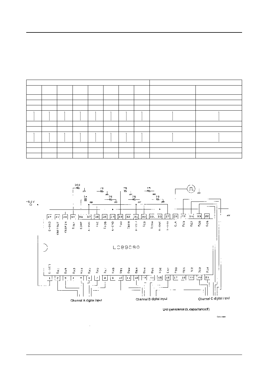
Sample Application Circuit: LC89080
No. 4030-5/8
LC89080, 89080Q
Digital input code
Analog output voltage
D1
D2
D3
D4
D5
D6
D7
D8
IO
IOB
MSB
LSB
(positive output)
(negative output)
0
0
0
0
0
0
0
0
0
0.996
0
0
0
0
0
0
0
1
0.004
0.992
0
0
0
0
0
0
1
0
0.008
0.988
0
1
1
1
1
1
1
1
0.496
0.500
1
0
0
0
0
0
0
0
0.500
0.496
1
1
1
1
1
1
0
1
0.988
0.008
1
1
1
1
1
1
1
0
0.992
0.004
1
1
1
1
1
1
1
1
0.996
0