 | –≠–ª–µ–∫—Ç—Ä–æ–Ω–Ω—ã–π –∫–æ–º–ø–æ–Ω–µ–Ω—Ç: LC89086M | –°–∫–∞—á–∞—Ç—å:  PDF PDF  ZIP ZIP |
Ordering number : EN
*
5428A
O3097HA (OT) No. 5428-1/6
Overview
The LC89086M is a low-power high-speed 8-bit serial-
parallel A/D converter fabricated in a high-speed CMOS
process.
Features
∑ Resolution: 8 bits (with an overflow output)
∑ Maximum conversion rate: 20M samples per second
∑ Error: Less than ±1.0 LSB
∑ Power supply: +5-V single-voltage power supply
∑ Power dissipation: 150 mW (typical)
∑ Analog input voltage range: V
SS
to V
DD
∑ Digital output voltage: 3 state TTL level
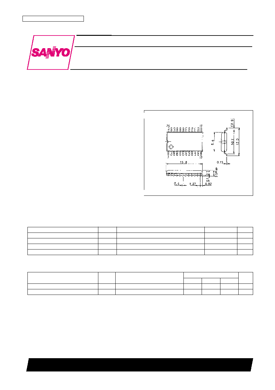
Package Dimensions
unit: mm
3155-MFP24
Preliminary
SANYO: MFP24
[LC89086M]
LC89086M
SANYO Electric Co.,Ltd. Semiconductor Bussiness Headquarters
TOKYO OFFICE Tokyo Bldg., 1-10, 1 Chome, Ueno, Taito-ku, TOKYO, 110 JAPAN
CMOS LSI
8 Bit A/D Converter
Parameter
Symbol
Conditions
Ratings
Unit
Maximum supply voltage
V
DD
max
≠0.3 to +7.0
V
Input voltage
V
IN
max
≠0.3 to V
DD
+0.3
V
Operating temperature
Topr
≠30 to +70
∞C
Storage temperature
Tstg
≠40 to +125
∞C
Specifications
Absolute Maximum Ratings
at Ta = 25∞C, DV
SS
= AV
SS
= 0 V
Parameter
Symbol
Conditions
Ratings
Unit
min
typ
max
Supply voltage
V
DD
4.5
5.0
5.5
V
Operating ambient temperature
Ta
≠30
+70
∞
C
Recommended Operating Conditions

No. 5428-2/6
LC89086M
Electrical Characteristics
Electrical DC Characteristics
at Ta = ≠30 to +70
∞
C, AV
DD
= DV
DD
= 4.5 to 5.5 V, AV
SS
= DV
SS
= 0 V
Parameter
Symbol
Conditions
Ratings
Unit
min
typ
max
Reference resistance
Rref
VrefH (pin 5) ≠ VrefL (pin 8)
210
300
390
Analog input capacitance
C
AIN
30
pF
Analog input resistance
R
AIN
10
M
Reference high-level input voltage
VrefH
When VrefHO (pin 4) and VrefLO (pin 9)
Vref L + 2.0
V
DD
V
are unused.
Reference low-level input voltage
VrefL
When VrefHO (pin 4) and VrefLO (pin 9) are unused.
0
VrefH ≠ 2.0
V
Reference high-level output voltage
VrefH
When VrefHO (pin 4) and VrefLO (pin 9)
1.9
2.0
2.1
V
are used, and AV
DD
= DV
DD
= 5 V
Reference low-level output voltage
VrefL
When VrefHO (pin 4) and VrefLO (pin 9)
≠0.05
0
+0.05
V
are used, and AV
DD
= DV
DD
= 5 V
Analog input voltage
V
AIN
VrefL
VrefH
V
Digital high-level voltage
V
IH
2.2
V
DD
+0.3
V
Digital low-level voltage
V
IL
≠0.3
+0.8
V
Digital high-level output current
I
OH
V
OH
= V
DD
≠ 0.4 V
≠2
mA
Digital low-level output current
I
OL
V
OL
= 0.4 V
2
mA
Parameter
Symbol
Conditions
Ratings
Unit
min
typ
max
Clock high-level period
T
WH
23
ns
Clock low-level period
T
WL
23
ns
Analog input acquisition time
T
AP
10
20
30
ns
Digital output data delay time
Td
C load = 30 pF
15
30
45
ns
Digital output data enable time
T
OE
C load = 30 pF
2
5
10
ns
Digital output data disable time
T
OD
C load = 30 pF
2
5
10
ns
Electrical AC Characteristics 1
at Ta = ≠30 to +70
∞
C, AV
DD
= DV
DD
= 4.5 to 5.5 V, AV
SS
= DV
SS
= 0 V
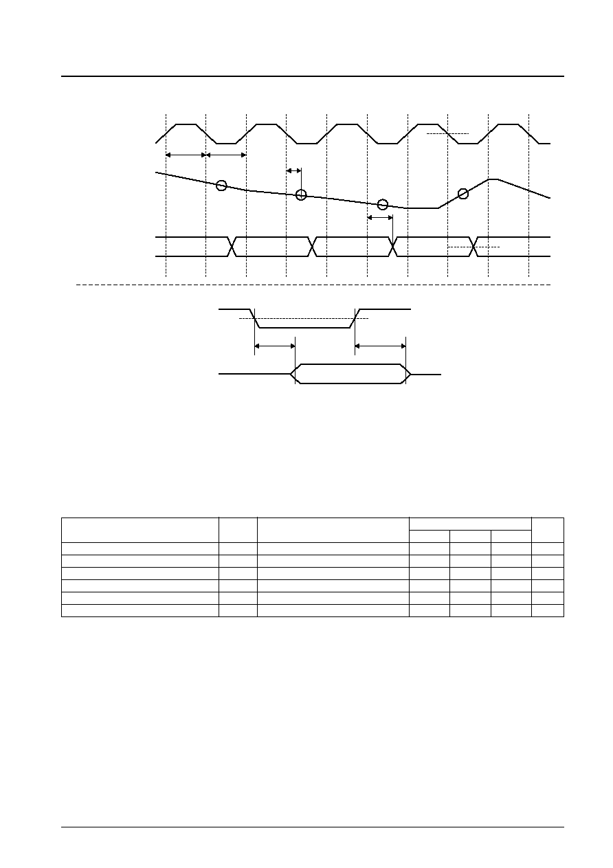
The analog signal (AIN) is acquired on the falling edge of the clock input (CLK). The acquired analog signal is
converted to a digital code and is output from the digital outputs (D8 to D1, OF) on the clock falling edge delayed three
clock cycles from the clock cycle in which the analog signal was acquired.
No. 5428-3/6
LC89086M
Timing Chart
TWH
TWL
TAP
Td
1.5 V
1.5 V
N
N + 1
N + 2
N + 3
N ≠ 4
N ≠ 3
N ≠2
N ≠ 1
N
Clock input
(CLK)
Analog input
(AIN)
Digital output
(D8 to D1,OF)
TOE
High impedance
1.5V
Output enable input
(OEB)
Digital output
(D8 to D1,OF)
TOD
A09018
Parameter
Symbol
Conditions
Ratings
Unit
min
typ
max
Resolution
Res
8
bit
Maximum conversion rate
Fs
20
MSPS
Linearity error
LE
DC accuracy
±1.0
LSB
Differential linearity error
DLE
DC accuracy
±1.0
LSB
Offset voltage
V
offset
DC accuracy
10
50
90
mV
Power dissipation
Pd
Fs = 20 MSPS
150
220
mW
Electrical AC Characteristics 2
at Ta = 25
∞
C, AV
DD
= DV
DD
= 5 V, AV
SS
= DV
SS
= 0 V, VrefH = 2 V, VrefL = 0 V
Note: Test circuits must conform to the sample application circuit.
No. 5428-4/6
LC89086M
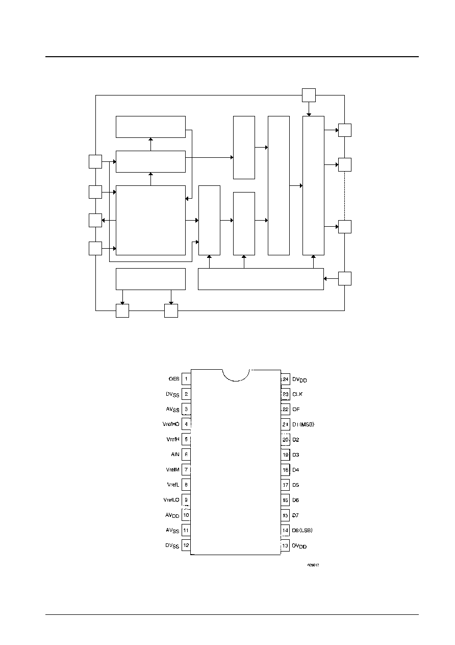
Block Diagram
Lower Vref selection
Upper comparator
Resistor string
Reference voltage
generation
Clock generation
5
VrefH
7
VrefM
8
VrefL
14
D8(LSB)
21
D1(MSB)
22
OF
23
CLK
4
VrefHO
1
OEB
9
VrefLO
6
AIN
Lower comparator
Lower encoder
Data correction
Output register
Upper encoder
A09019
Pin Assignment
Top view
No. 5428-5/6
LC89086M
Pin Functions
Pin No.
Pin name
I/O
Function
Digital output enable input
1
OEB
I
High: high-impedance
Low: Normal operation
2
DV
SS
Digital ground
3
AV
SS
Analog ground
4
Vref HO
O
Internal reference voltage (high) generation. Shorting this pin to VrefH (pin 5) generates a voltage of 2.0 V.
This pin must be left open when the internally generated potential is not used.
5
Vref H
I
Reference voltage input (high)
6
AIN
I
Analog input
7
Vref M
O
Reference voltage intermediate level tap.
8
Vref L
I
Reference voltage input (low)
9
Vref LO
O
Internal reference voltage (low) generation. Shorting this pin to VrefL (pin 8) generates a voltage of 0 V.
This pin must be left open when the internally generated potential is not used.
10
AV
DD
Analog power supply
11
AV
SS
Analog ground
12
DV
SS
Digital ground
13
DV
DD
Digital power supply
14
D8
O
Digital output (LSB)
15
D7
O
Digital output
16
D6
O
Digital output
17
D5
O
Digital output
18
D4
O
Digital output
19
D3
O
Digital output
20
D2
O
Digital output
21
D1
O
Digital output (MSB)
22
OF
O
Digital output (Overflow)
23
CLK
I
Clock input
24
DV
DD
Digital power supply
Note: There must be no potential difference between the digital system and analog system V
DD
and V
SS
power supply potentials.
I/O Code Table
The table below lists the relationship between the input and output when VrefH and VrefL are set up so that the zero
transient voltage is 0.000 V and the full-scale transient voltage is 2.008V.
Analog input
Digital output
V
AIN
(V)
OF
D1
D2
D3
D4
D5
D6
D7
D8
Up to 0.000
0
0
0
0
0
0
0
0
0
Up to 0.008
0
0
0
0
0
0
0
0
0
Up to 0.016
0
0
0
0
0
0
0
0
1
Up to 0.024
0
0
0
0
0
0
0
1
0
Up to 0.032
0
0
0
0
0
0
0
1
1
to
Up to 0.992
0
0
1
1
1
1
1
1
0
Up to 1.000
0
0
1
1
1
1
1
1
1
Up to 1.008
0
1
0
0
0
0
0
0
0
Up to 1.016
0
1
0
0
0
0
0
0
1
to
Up to 1.992
0
1
1
1
1
1
1
0
1
Up to 2.000
0
1
1
1
1
1
1
1
0
Up to 2.008
0
1
1
1
1
1
1
1
1
Over 2.008
1
1
1
1
1
1
1
1
1