 | –≠–ª–µ–∫—Ç—Ä–æ–Ω–Ω—ã–π –∫–æ–º–ø–æ–Ω–µ–Ω—Ç: LC89210 | –°–∫–∞—á–∞—Ç—å:  PDF PDF  ZIP ZIP |
Overview
The LC89210 is a highly integrated modem engine that
can be used in products that support transmission rates up
to the 14,400 bps rate used in contemporary group III fax
equipment. The LC89210 is compatible with V.21, V.23
and Bell 103 full-duplex modems.
Features
∑ Supports the ITU-T V.17, V.29, and V.27ter fax
standards
∑ ITU-T V.23, V.21, and Bell 103
∑ V.17, V.29 (T104), and V.27ter short training
∑ V.33 half duplex
∑ 1800-Hz or 1700-Hz carrier
∑ The LC89210 is a complete data pump on a single chip.
∑ 5 V single-voltage power supply
-- Operating power dissipation: 375 mW (typical)
-- Low power mode: 5 mW (typical)
∑ Expanded operating modes
-- Full implementation of V.17, V.33, V.29, and
V.27ter handshaking
-- Autodial and autoanswer functions
-- Programmable tone detection and FSK V.21 flag
pattern detection during high-speed reception
-- Programmable call progresss and call waiting tone
detection, including DTMF
-- Support for programmable CLASS
TM
detection
-- Wide dynamic range (better than 48 dB)
-- A-law voice PCM mode
∑ Multiple interfaces
-- Parallel 64
◊
8-bit dual-port RAM
-- Synchronous/HDLC parallel data processing
-- Support for HDLC framing
-- V.24 interface
-- Can monitor all operating states in real time.
-- Includes all diagnostic functions.
-- Dual 8-bit D/A converter for eye pattern display
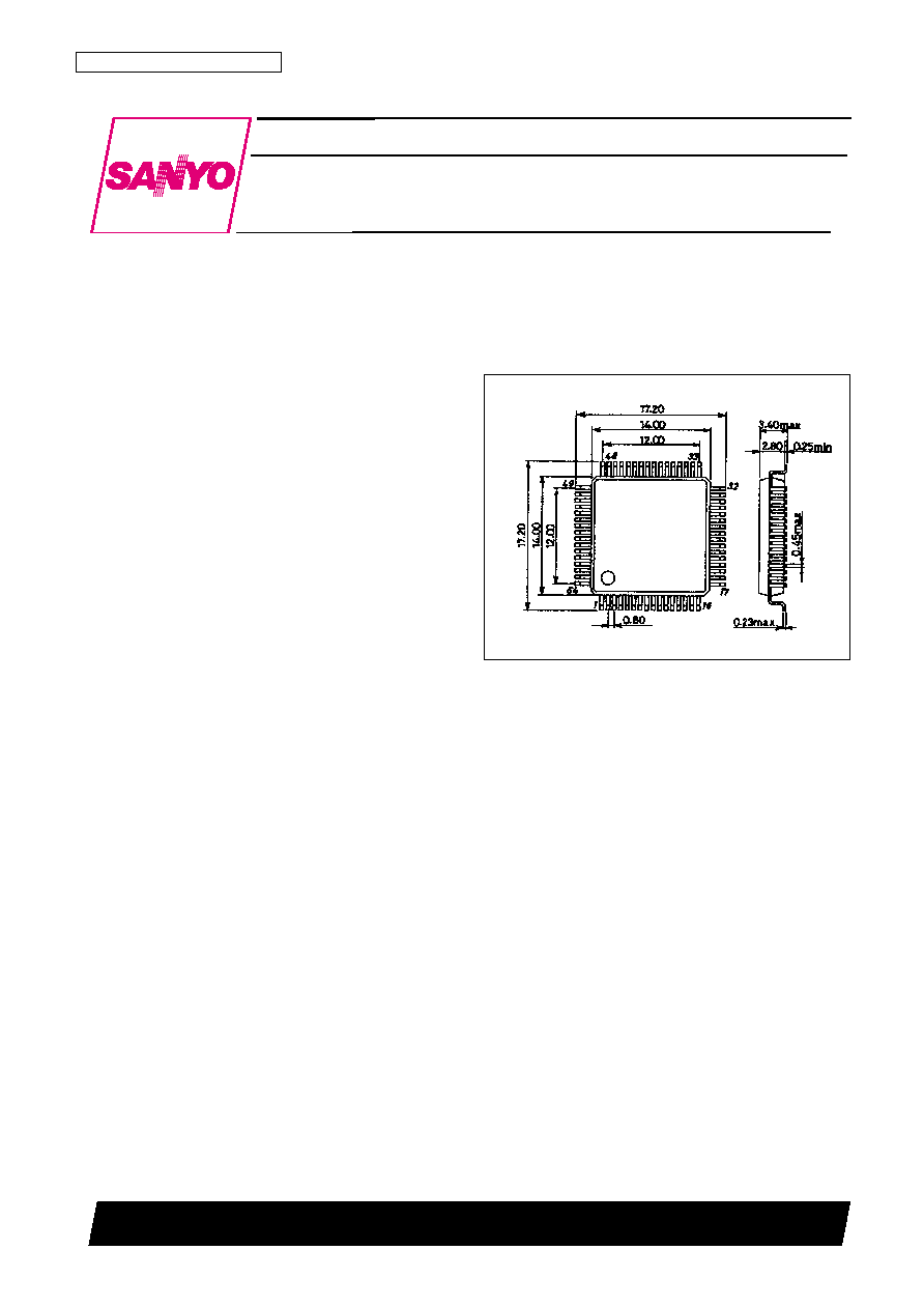
Package Dimensions
unit: mm
3213-PQFP64
CMOS LSI
52696HA (OT) No. 5382-1/10
Preliminaly
SANYO: PQFP64
[LC89210]
SANYO Electric Co.,Ltd. Semiconductor Bussiness Headquarters
TOKYO OFFICE Tokyo Bldg., 1-10, 1 Chome, Ueno, Taito-ku, TOKYO, 110 JAPAN
High-speed fax modem data pump
LC89210
Ordering number : EN
*
5382

No. 5382-2/10
LC89210
Specifications
Electrical Specifications
at Ta = 25∞C, V
DD
= 5 V (unless otherwise specified)
Absolute Maximum Ratings
with respect to ground
Electrical Characteristics
at Ta = 0 to +70∞C, V
DD
= 5.0 V ± 5%, GND = 0 V (unless otherwise specified)
Parameter
Symbol
Conditions
Ratings
Unit
DC supply voltage
V
DD
≠0.3 to +7.0
V
Digital or analog input voltage
V
I
, V
IN
≠0.3 to (V
DD
+ 0.3)
V
Digital or analog input current
I
I
, I
IN
±1
mA
Digital output current
I
O
±20
mA
Analog output current
I
OUT
±10
mA
Allowable power dissipation
Pd max
1000
mW
Operating temperature
Topr
0 to +70
∞C
Storage temperature (plastic)
Tstg
≠40 to +125
∞C
Parameter
Symbol
Conditions
min
typ
max
Unit
[Power Supply and Common-Mode Voltages]
Supply voltage
V
DD
4.75
5
5.25
V
Current drain
I
DD
75
100
mA
Current drain in lower power mode
I
DD-ip
1
mA
Common-mode voltage
V
CM
V
DD
/2 ≠ 5%
V
DD
/2
V
DD
/2 + 5%
V
[Crystal Oscillator Interface] XTAL and EXTAL
Input low-level voltage
V
IL
1.5
V
Input high-level voltage
V
IH
3.5
V
Input low-level current
I
L
GND < V
I
< V
IL
max
≠15
µA
Input high-level current
I
H
V
IH
min < V
I
< V
DD
15
µA
[Digital Interface] All digital pins except the XTAL pin
Input low-level voltage
V
IL
≠0.3
+0.8
V
Input high-level voltage
V
IH
2.2
V
Input current
I
I
V
I
= V
DD
or V
I
= GND
≠10
0
+10
µA
Output high-level voltage
V
OH
I
lord
= 2 mA
2.4
V
Output low-level voltage
V
OL
I
lord
= 2 mA
0.4
V
3-state input leakage current
I
OZ
GND < V
O
< V
DD
≠50
0
+50
µA
Input capacitance
C
IN
5
pF
[Analog Interface]
Differential reference voltage input
V
REF
V
REFP
≠ V
REFN
2.40
2.50
2.60
V
Input common-mode offset
V
CMOin
V = (RXA1 + RXA2)/2 ≠ V
CM
≠300
+300
mV
Differential input voltage
V
DIFin
RXA1 ≠ RXA2
2
◊
V
REF
Vp-p
Output common-mode
V
CMOout
(TXA1 + TXA2)/2 ≠ V
CM
≠200
+200
mV
voltage offset
Differential output voltage
V
DIFout
TXA1 ≠ TXA2
2
◊
V
REF
Vp-p
Differential output DC offset
V
OFFout
(TXA1 ≠ TXA2)
≠100
+100
mV
Input resistance
Rin
RXA
X
100
k
Output resistance
Rout
TXA
X
20
Load resistance
R
L
TXA
X
10
k
Load capacitance
C
L
TXA
X
50
pF

No. 5382-3/10
LC89210
Pin Assignment
Host Interface
The LC89210 is interfaced to the control processor through a 64-byte dual-port RAM that is shared by the LC89210 and
the host.
Note:
*
Open-drain output
Pin
Type
Function
SD0 to SD7
I/O
System data bus
SA0 to SA6
I
System address bus
SDS (SDR)
I
System data strobe
SR/W (SWR)
I
System read/write
SCS
I
System chip select
SDTACK
OD
*
System bus data acknowledge
SINTR
OD
*
System interrupt request
RESET
I
Reset. This is an active-low signal.
RING
I
Ring detect signal
INT/MOT
I
Intel/Motorola interface

No. 5382-4/10
LC89210
Analog Interface
V.24 Interface
Other Interfaces
Note: The LC89210 nominal external clock frequency is 29.4912 MHz. This value has a precision of ±5.10
≠5
.
Boundary Scan Interface
The LC89210 provides 13 signals for testing. These signals can be used along with the SGS-Thomson ST18932
boundary scan development tools in the product development process to debug application hardware and software. If this
function is not used, all of these input signal must be connected to ground, and all of these output signals must be left
open.
Pin
Type
Function
TXA1
O
Transmission analog output 1
TXA2
O
Transmission analog output 2
RXA1
I
Reception analog input 1
RXA2
I
Reception analog input 2
V
CM
I/O
Analog common voltage (nominal value: +2.5 V)
V
REFN
I
Analog negative reference voltage (nominal value: CM ≠ 1.25 V)
V
REFP
I
Analog positive reference voltage (nominal value: CM + 1.25 V)
Pin
Type
Function
RTS
I
Transfer request. This is an active-low signal.
CLK
O
Data bit clock
CTS
O
Clear to send. This is an active-low signal.
RXD
O
Reception data
TXD
I
Transfer data
CD
O
Carrier detect. This is an active-low signal.
Pin
Type
Function
XTAL
O
Internal oscillator output
EXTAL
I
Internal oscillator input or external clock
EYEX
O
Constellation X analog coordinate (eye pattern)
EYEY
O
Constellation Y analog coordinate (eye pattern)
TEST1
This pin must be left open
TEST2
This pin must be left open
Pin
Type
Function
SCIN
I
Scan data input
SCCLK
I
Scan clock
SCOUT
O
Scan data output
BOS
I
Scan control start
EOS
I
Scan stop
MC0 to MC2
I
Mode control
HALT
I
LC89210 execution step
MC1
O
Multi-cycle instruction
RDYS
O
Scan flag ready
EBS
I
Enable boundary scan
CLKOUT
O
LC89210 internal clock (the crystal oscillator frequency divided by 2)
No. 5382-5/10
LC89210
Power Supply
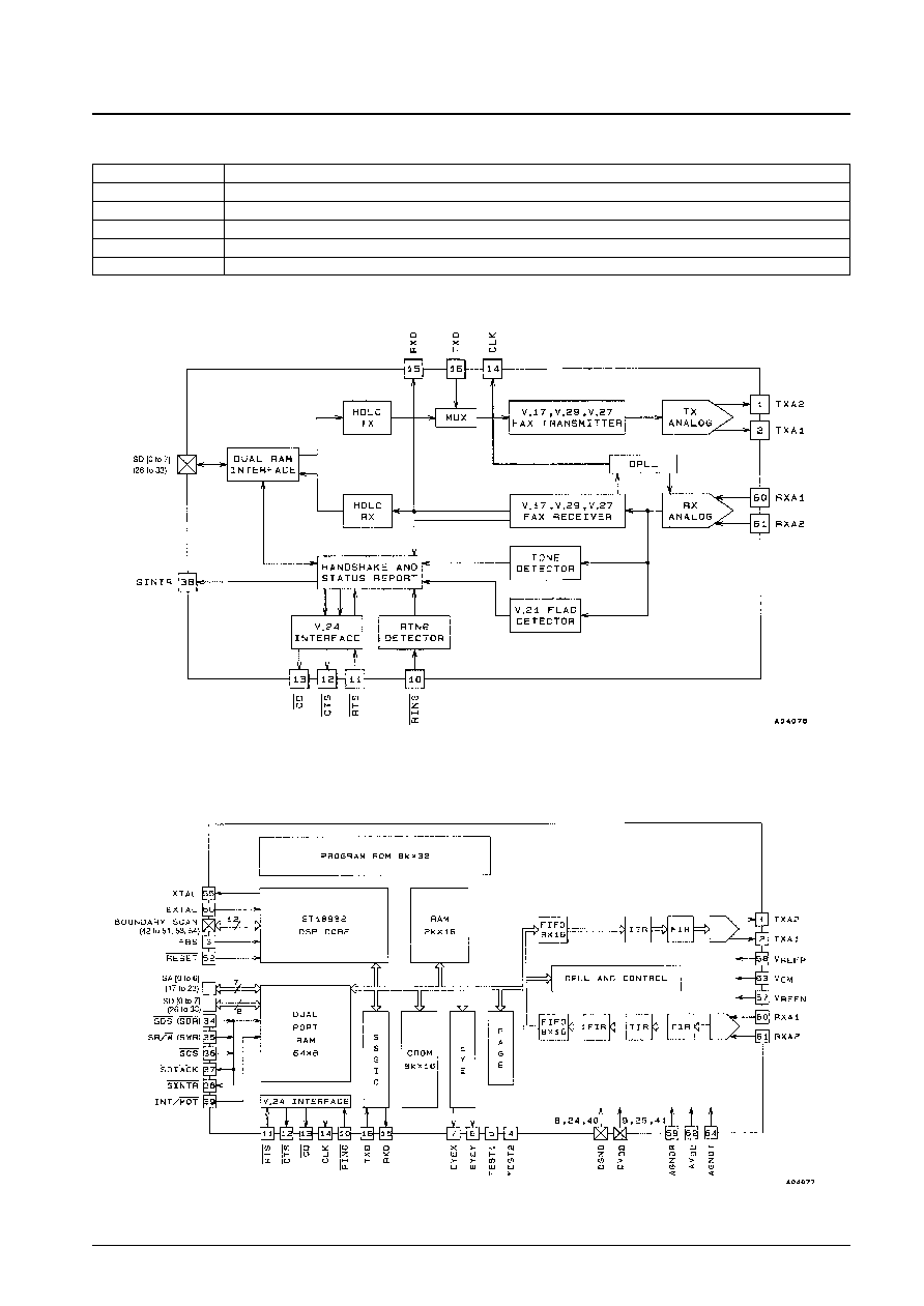
Block Diagrams
Function Block Diagram
Hardware Block Diagram
Symbol
Parameter
V
DD
Digital +5 V (pins 9, 25, and 41)
GND
Digital ground (pins 8, 24, and 40)
AV
DD
Analog +5 V (pin 62)
AGNDT
Analog transmission system ground (pin 64)
AGNDR
Analog reception system ground (pin 59)