 | –≠–ª–µ–∫—Ç—Ä–æ–Ω–Ω—ã–π –∫–æ–º–ø–æ–Ω–µ–Ω—Ç: LC895127K | –°–∫–∞—á–∞—Ç—å:  PDF PDF  ZIP ZIP |
Ordering number : ENN6236
D1599TH (OT)/30899TH (OT) No. 6236-1/8
Functions
∑ CD-ROM ECC function
∑ SCSI I/F function
∑ Subcode I/F function
∑ CAV audio function
Features
∑ SCSI interface (includes on-chip SCAM selection register)
∑ Supports 20
◊
speed and a 10 MBytes/s transfer rate
when using 16-bit 70-ns EDO DRAM
∑ Supports 40
◊
speed and a 10 MB/s transfer rate
when using 16-bit 50-ns EDO DRAM
∑ Up to 4 M bits of buffer RAM can be used.
∑ The user can freely set up the CD main channel and the
C2 flag areas in buffer RAM.
∑ Batch transfer function (Allows the CD main channel, the
C2 flags, and other data to be sent in a single operation.)
∑ Multi-block transfer function (Allows multiple blocks to
be sent automatically in a single operation.)
∑ Subcode buffering and CD-TEXT support
∑ CAV audio function
∑ Supports 20 MBytes/s transfers
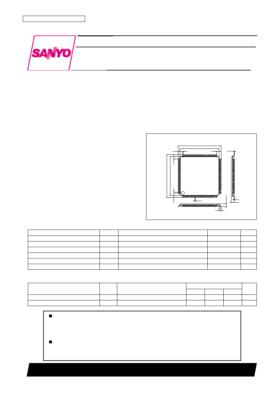
∑ Package: SQFP-144
Package Dimensions
unit: mm
3214-SQFP144
LC895127, 895127K
SANYO Electric Co.,Ltd. Semiconductor Company
TOKYO OFFICE Tokyo Bldg., 1-10, 1 Chome, Ueno, Taito-ku, TOKYO, 110-8534 JAPAN
40
◊
CD-ROM Decoder with SCSI Interface
CMOS IC
Parameter
Symbol
Conditions
Ratings
Unit
Maximum supply voltage
V
DD
max
Ta = 25∞C
≠0.3 to +7.0
V
Input/output voltage
V
I
, V
O
Ta = 25∞C
≠0.3 to V
DD
+ 0.3
V
Allowable power dissipation
Pd max
Ta
70∞C
550
mW
Operating temperature
Topr
≠30 to +70
∞C
Storage temperature
Tstg
≠55 to +125
∞C
Soldering temperature (pin part only)
10 s
260
∞C
Specifications
Absolute Maximum Ratings
at V
SS
= 0 V
Allowable Operating Ranges
at Ta = ≠30∞C to +70∞C, V
SS
= 0 V
Parameter
Symbol
Conditions
Ratings
Unit
min
typ
max
Supply voltage
V
DD
4.5
5.0
5.5
V
Input voltage range
V
IN
0
V
DD
V
0.20
1.25
1.25
22.0
20.0
0.5
22.0
20.0
0.5
1.25
1.25
0.145
0.1
1.4
1.6max
0.5
0.5
1
36
37
72
73
108
109
144
SANYO: SQFP144
[LC895127, 895127K]
Any and all SANYO products described or contained herein do not have specifications that can handle
applications that require extremely high levels of reliability, such as life-support systems, aircraft's
control systems, or other applications whose failure can be reasonably expected to result in serious
physical and/or material damage. Consult with your SANYO representative nearest you before using
any SANYO products described or contained herein in such applications.
SANYO assumes no responsibility for equipment failures that result from using products at values that
exceed, even momentarily, rated values (such as maximum ratings, operating condition ranges, or other
parameters) listed in products specifications of any and all SANYO products described or contained
herein.
No. 6236-2/8
LC895127, 895127K
Applicable pin sets are as follows.
INPUT
(1)
TEST0 to TEST4, CSCTRL, SUA0 to SUA6, C2P0, SDATA, BCK, LRCK, SCOR, WFCK, SBS0, MCK2SEL
(2)
RESET
(3)
CS, RD, WR
(4)
SCSISEL, XTALSEL
OUTPUT
(5)
INT0, INT1, SWAIT
(6)
MCK
(7)
EXCK, DSDATA, DLRCK, DBCK, RAS0, CAS0, CAS1, OE, UWE, LWE, RA0 to RA8
INOUT
(8)
ACK, ATN
(9)
D0 to D7, IO0 to IO15, IOP0 to IOP7
(10) DB0 to DB7, DBP, BSY, I/O, MSG, SEL, RST, REQ, C/D
(11) IOP0 to IOP7
Note: Pins XTAL0, XTALCK0, XTAL1, XTALCK1, and X1EN are not included in DC characteristics.
Parameter
Symbol
Conditions
Applicable pins
Ratings
Unit
min
typ
max
Input high-level voltage
V
IH1
TTL levels
(1)
2.2
V
Input low-level voltage
V
IL1
0.8
V
Input high-level voltage
V
IH2
TTL levels
(9)
2.2
--
--
V
Input low-level voltage
V
IL2
with pull-up resistor
--
--
0.8
V
Input high-level voltage
V
IH3
TTL levels
(2)
2.2
--
--
V
Input low-level voltage
V
IL3
Schmitt
--
--
0.8
V
Input high-level voltage
V
IH4
CMOS levels
(3)
0.8 V
DD
--
--
V
Input low-level voltage
V
IL4
Schmitt
--
--
0.2 V
DD
V
Input high-level voltage
V
IH5
(4), (8), (10)
2.0
--
V
Input low-level voltage
V
IL5
0.8
V
Input high-level voltage
V
IH2
TTL levels
(11)
2.2
--
V
Input low-level voltage
V
IL2
with pull-up resistor
--
--
0.8
V
Output high-level voltage
V
OH1
I
OH1
= ≠12 mA
(6)
V
DD
≠ 2.1
--
--
V
Output low-level voltage
V
OL1
I
OL1
= 12 mA
--
--
0.4
V
Output high-level voltage
V
OH2
I
OH2
= ≠8 mA
(7)
2.4
V
Output low-level voltage
V
OL2
I
OL2
= 8 mA
0.4
V
Output high-level voltage
V
OH2
I
OH2
= ≠2 mA
(9), (5), (11)
2.4
V
Output low-level voltage
V
OL2
I
OL2
= 2 mA
0.4
V
Output low-level voltage
V
OL4
I
OL4
= 48 mA
(10)
0.4
V
Input leakage current
I
IL
V
I
= V
SS
, V
DD
All input pins
≠25
+25
µA
Pull-up resistance
R
UP
(5), (9), (11)
60
120
240
k
DC Characteristics
at Ta = ≠30 to +70∞C, V
SS
= 0 V, V
DD
= 4.5 to 5.5 V
No. 6236-3/8
LC895127, 895127K
Parameter
Symbol
Conditions
Ratings
Unit
min
typ
max
Output high-level voltage
V
OH
2.5
V
Output low-level voltage
V
OL
0.4
V
Active-Low Output Characteristics
SCSI Pin Input Characteristics
Parameter
Symbol
Conditions
Ratings
Unit
min
typ
max
Input threshold voltage
V
t+t1
V
DD
= 4.50 to 5.50 V
1.60
2.00
V
V
t≠t1
0.80
1.10
V
Hysteresis width
V
tt1
V
DD
= 5.0 V
0.41
0.5
V
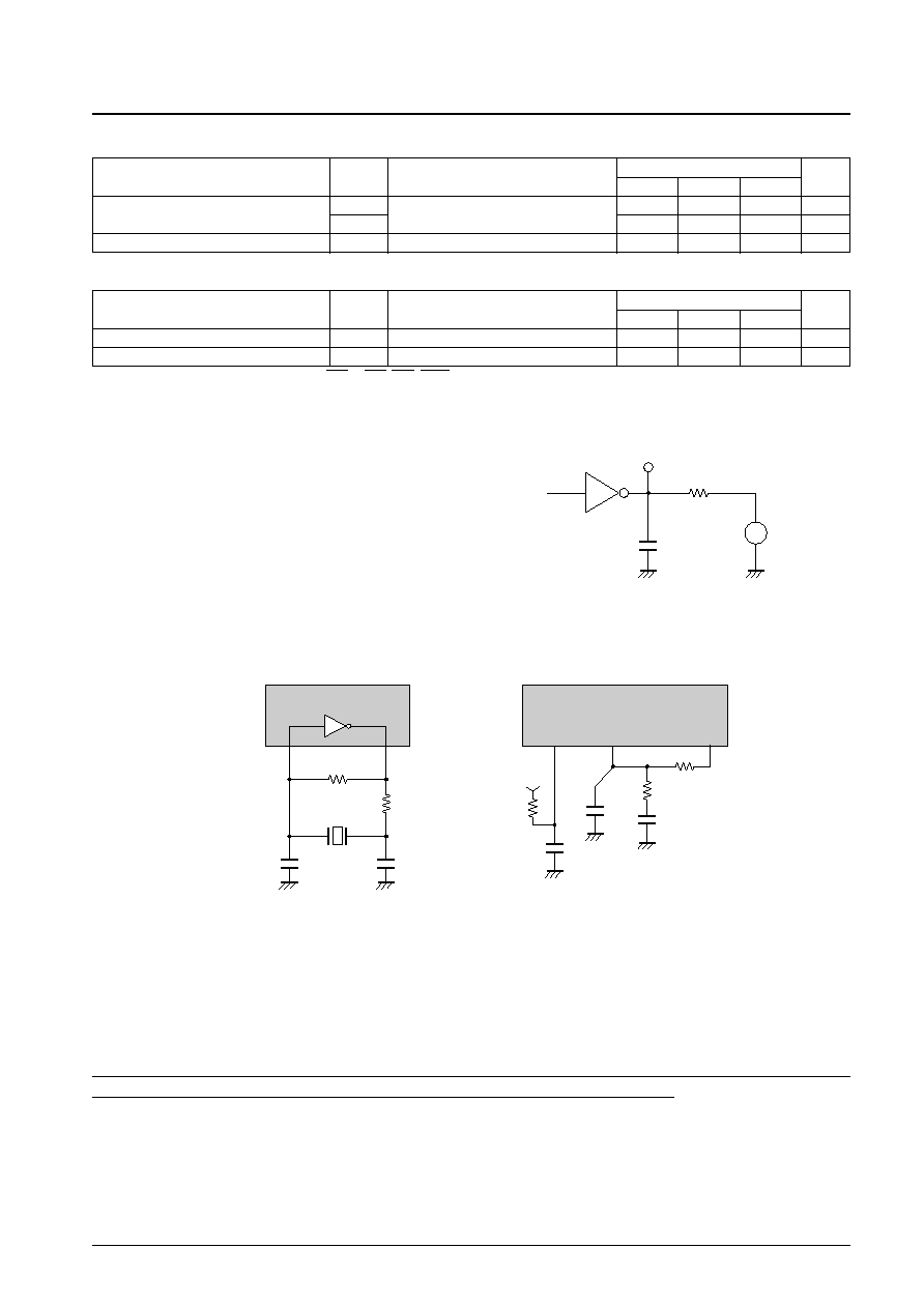
Note: Only applies to the active-low output pins DB0 to DB7, REQ, DBPB
SCSI
driver
TP
47
±
5 %
15 pF
±
5 %
2.5 V
+
≠
A12526
Rise time test circuit
Recommended Oscillator and PLL Circuits
LC895127
R1
R2
C2
C1
XTALCK0
PN27
XTAL0
PN28
PN69
PN70
PN71
A12527
LC895127
PLL
R5
R4
C3
C4
C5
R3
A12528
R1 = 120 k
, R2 = 47
, C1 = 30 pF
Crystal oscillator frequency XTALCK0 = 16.9344 MHz
R3 = 7.5 k
, R4 = 200
, R5 = 10 k
, C3 = 0.1 µF
C4 = 0.1 µF, C5 = 0.002 µF to 0.01 µF
Note: The values listed above for R3, R4, R5, and C3 also apply when the XTALKC0 frequency is 33.8688 MHz.
Applications must be designed so that the analog V
DD
and V
SS
power supply system is completely independent of the
logic system power supply and is not affected by the logic system power supply fluctuation in any way.
Note: Since the exact values of these components will vary depending on the characteristics of the printed circuit board
used and other factors, consult the manufacturer of the crystal element when designing the oscillator circuit.
No. 6236-4/8
LC895127, 895127K
Pin Functions
Type
I
INPUT
B
BIDIRECTION
NC
NOT CONNECT
O
OUTPUT
P
POWER
Pin No.
Pin name
Type
Pin functions
1
V
SS0
P
2
IO2
B
Buffer RAM data I/O
3
IO1
B
These pins have built-in pull-up resistors.
4
IO0
B
5
MCK2SEL
I
PLL frequency selection. Currently, this pin must be connected to V
DD
.
6
C2PO
I
7
SDATA
I
CD DSP interface
8
BCK
I
9
LRCK
I
10
EXCK
O
Subcode I/O
11
WFCK
I
12
SBSO
I
Subcode I/O
13
SCOR
I
14
DSDATA
O
15
DLRCK
O
D/A converter outputs
16
DBCK
O
17
MCK
O
XTALCLK0 1/1, 1/2, and stop output
18
V
DD
P
19
V
SS0
P
20
RESET
I
IC reset. The IC is reset on a low-level input
21
CSCTRL
I
MC (Microcontroller) CSL
0
, Hi
22
TEST3
I
23
TEST0
I
Test pins. These pins must be connected to V
SS0
in normal operation.
24
TEST1
I
25
TEST2
I
26
V
SS0
P
27
XTALCK0
I
Crystal oscillator circuit input
28
XTAL0
O
Crystal oscillator circuit output
29
TEST4
I
Test pin. This pin must be connected to V
SS0
in normal operation.
30
V
SS0
P
31
V
SS0
P
32
V
SS0
P
33
V
SS0
P
34
IOP7
I
General-purpose I/O ports. These pins include built-in pull-up resistors.
35
IOP6
I
36
V
SS0
P
37
V
DD
P
38
IOP5
I
39
IOP4
I
40
IOP3
I
General-purpose I/O ports. These pins include built-in pull-up resistors.
41
IOP2
I
42
IOP1
I
43
IOP0
I
44
V
SS0
P
45
RD
I
Microcontroller data read signal input
46
WR
I
Microcontroller data write signal input
47
CS
I
Register chip select input from the microcontroller
48
SUA0
I
49
SUA1
I
50
SUA2
I
Microcontroller register selection signals
51
SUA3
I
52
SUA4
I
53
SUA5
I
Continued on next page.

No. 6236-5/8
LC895127, 895127K
Continued from preceding page.
Pin No.
Pin
I/O
Function
54
V
DD
P
55
V
SS0
P
56
SUA6
I
Microcontroller register selection signals
57
D0
B
58
D1
B
59
D2
B
Microcontroller data signals
60
D3
B
61
D4
B
62
D5
B
63
V
SS0
P
64
D6
B
Microcontroller data signals
65
D7
B
66
INT0
O
Interrupt request signal output to the microcontroller (ECC side. Set by setting a register value.)
67
INT1
O
Interrupt request signal output to the microcontroller (SCSI side. Set by setting a register value.)
68
SWAIT
O
Wait signal output to the microcontroller
69
X1EN
I
Used by the PLL. This pin must be connected to V
DD
through a resistor.
70
XTALCK1
I
Used by the PLL.
71
XTAL1
O
Used by the PLL.
72
V
SS0
P
Analog V
SS
73
V
DD
P
Analog V
DD
74
NC
75
I/O
B
SCSI interface
76
REQ
B
77
V
SS1
P
78
C/D
B
SCSI interface
79
SEL
B
80
NC
81
V
DD
P
82
V
SS1
P
83
MSG
B
SCSI interface
84
RST
B
85
V
SS1
P
86
ACK
B
SCSI interface
87
BSY
B
88
V
SS1
B
89
ATN
B
SCSI interface
90
V
DD
P
91
V
SS1
P
92
NC
93
DBP
B
SCSI interface
94
V
DD
P
95
DB7
B
SCSI interface
96
DB6
B
97
V
SS1
P
98
DB5
B
SCSI interface
99
DB4
B
100
V
DD
P
101
DB3
B
SCSI interface
102
DB2
B
103
V
SS1
P
104
DB1
B
SCSI interface
105
DB0
B
106
SCSISEL
I
SCSI pin layout selection. (This pin must be connected to V
SS0
.)
107
XTALSEL
I
PLL XTAL oscillator selection
Continued on next page.