 | –≠–ª–µ–∫—Ç—Ä–æ–Ω–Ω—ã–π –∫–æ–º–ø–æ–Ω–µ–Ω—Ç: LC895194 | –°–∫–∞—á–∞—Ç—å:  PDF PDF  ZIP ZIP |
CMOS LSI
Ordering number : EN
*
5154B
N3097HA(OT) /81095HA (OT) No. 5154-1/7
Preliminary
SANYO Electric Co.,Ltd. Semiconductor Bussiness Headquarters
TOKYO OFFICE Tokyo Bldg., 1-10, 1 Chome, Ueno, Taito-ku, TOKYO, 110 JAPAN
CD-ROM Error Correction LSI
with On-Chip ATA-PI (IDE) Interface
LC895194
Functions
CD-ROM error detection and correction, ATA-PI (IDE)
interface (including the register and other blocks)
Features
∑ ATA-PI (IDE) interface
∑ Supports 16
◊
-speed playback (with IORDY): Using 16
◊
70 ns DRAMs
∑ 16.6 MB/s transfer rate: Using 16
◊
70 ns DRAMs
∑ Supports the use of from 1 M to 32 M of buffer RAM.
(DRAM)
∑ Allows the user to arbitrarily set the CD main channel
and C2 flag areas in buffer RAM.
∑ Batch transfer function (function for transferring the CD
main channel and C2 flag data in one operation)
∑ Multi-transfer function (function for sending multiple
blocks in one operation)
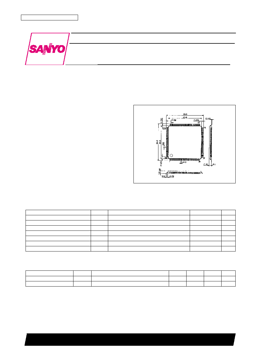
Package Dimensions
unit: mm
3214-SQFP144
Specifications
Absolute Maximum Ratings
at V
SS
= 0 V
Note:
*
Per cell for basic I/O cells
Allowable Operating Ranges
at Ta = ≠30 to +75∞C, V
SS
= 0 V
Parameter
Symbol
Conditions
Ratings
Unit
Maximum supply voltage
V
DD
max
Ta = 25∞C
≠0.3 to +7.0
V
I/O voltages
V
I
, V
O
Ta = 25∞C
≠0.3 to V
DD
+ 0.3
V
Allowable power dissipation
Pd max
Ta
70∞C
550
mW
Operating temperature
Topr
≠30 to +75
∞C
Storage temperature
Tstg
≠55 to +125
∞C
Soldering heat resistances (pins only)
10 seconds
235
∞C
I/O power
I
I
, I
O
±20
*
mA
Parameter
Symbol
Conditions
min
typ
max
Unit
Supply voltage
V
DD
4.5
5.0
5.5
V
Input voltage range
V
IN
0
V
DD
V
[LC895194]
SANYO: SQFP144

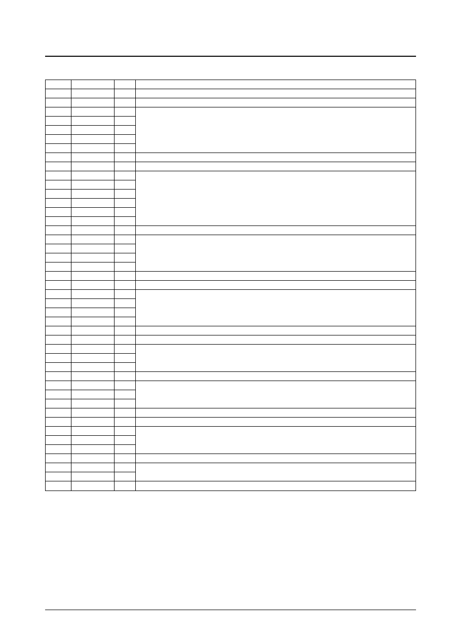
DC Characteristics
at V
SS
= 0 V, V
DD
= 4.5 to 5.5 V, Ta = ≠30 to +75∞C
Note:
*
The entries in the "Applicable Pins" column specify the following pin sets.
[Input]
1: CSCTRL, SUA0 to SUA6
2: TEST0 to TEST4
3: DA0 to DA2, ZCS1FX, ZCS3FX, ZDIOR, ZDIOW, ZDMACK, ZHRST, ZRESET, BCK, C2PO, LRCK, SDATA
4: ZCS, ZRD, ZWR
5: WFCK, SCOR
[Output]
6: ZINT1
7: MCK, MCK2
8: ZINT, ZSWAIT
9: DMARQ, HINTRQ
10: RA0 to RA9, ZCAS0, ZCAS1, ZLWE, ZOE, ZRAS0, ZRAS1, ZUWE
11: ZRSTCPU, ZRSTIC
12: IORDY, ZIOCS16
[I/O]
13: D0 to D7, IO0 to IO15
14: DD0 to DD15, ZDASP, ZPDIAG
Note: XTAL, XTALCK
The above pins are not included in the DC characteristics.
Sample Recommended Oscillator Circuit
R1 = 120 k
R2 = 47 k
C1 = 30 pF
For a crystal oscillator frequency of 16.9344 MHz.
Alternatively:
R1 = 3.3 k
R2 = None
C1 = 5 pF
For a crystal oscillator frequency of 33.8688 MHz.
For an oscillator frequency of 33.8688, the third harmonic is used. This means that
precise component values will be influenced by the printed circuit board. Consult
the manufacturer of the crystal to determine the circuit constants for this frequency.
No. 5154-2/7
LC895194
Parameter
Symbol
Applicable Pins
* (
See below
)
min
typ
max
Unit
Input high level voltage
V
IH
TTL compatible: (1)
2.2
--
--
V
Input low level voltage
V
IL
--
--
0.8
V
Input high level voltage
V
IH
TTL compatible, with pull-up resistor: (13)
2.2
--
--
V
Input low level voltage
V
IL
--
--
0.8
V
Input high level voltage
V
IH
TTL compatible, with pull-down resistor: (2)
2.2
--
--
V
Input low level voltage
V
IL
--
--
0.8
V
Input high level voltage
V
IH
TTL compatible, Schmitt: (3), (5), and (14)
2.4
--
--
V
Input low level voltage
V
IL
--
--
0.8
V
Input high level voltage
V
IH
COMS compatible, Schmitt: (4)
0.8 V
DD
--
--
V
Input low level voltage
V
IL
--
--
0.2 V
DD
V
Output high level voltage
V
OH
I
OH
= ≠2 mA
(8), (10), and (13)
V
DD
≠ 2.1
--
--
V
Output low level voltage
V
OL
I
OL
= 2 mA
--
--
0.4
V
Output high level voltage
V
OH
I
OH
= ≠8 mA
(7)
V
DD
≠ 2.1
--
--
V
Output low level voltage
V
OL
I
OL
= 8 mA
--
--
0.4
V
Output high level voltage
V
OH
I
OH
= 4 mA
(9), and (14)
V
DD
≠ 2.1
--
--
V
Output low level voltage
V
OL
I
OL
= 24 mA
--
--
0.4
V
Output high level voltage
V
OH
I
OH
= ≠2 mA
(6)
V
DD
≠ 2.1
--
--
V
Output low level voltage
V
OL
I
OL
= 2 mA
--
--
0.4
V
Output low level voltage
V
OL
I
OL
= 2 mA
(11)
--
--
0.4
V
Output low level voltage
V
OL
I
OL
= 24 mA
(12)
--
--
0.4
V
Input leakage current
I
IL
V
I
= V
SS
, V
DD
: (1), (3), (4), (9), and (14)
≠10
--
+10
µA
Output leakage current
I
OZ
For high-impedance outputs: (6), (12), and (14)
≠10
--
+10
µA
Pull-up resistance
R
UP
(13)
40
80
160
k
Pull-down resistance
R
DN
(2), (5)
40
80
160
k
Input voltage hysteresis
V
HYS
(3), and (14)
0.8
1.0
1.3
mV
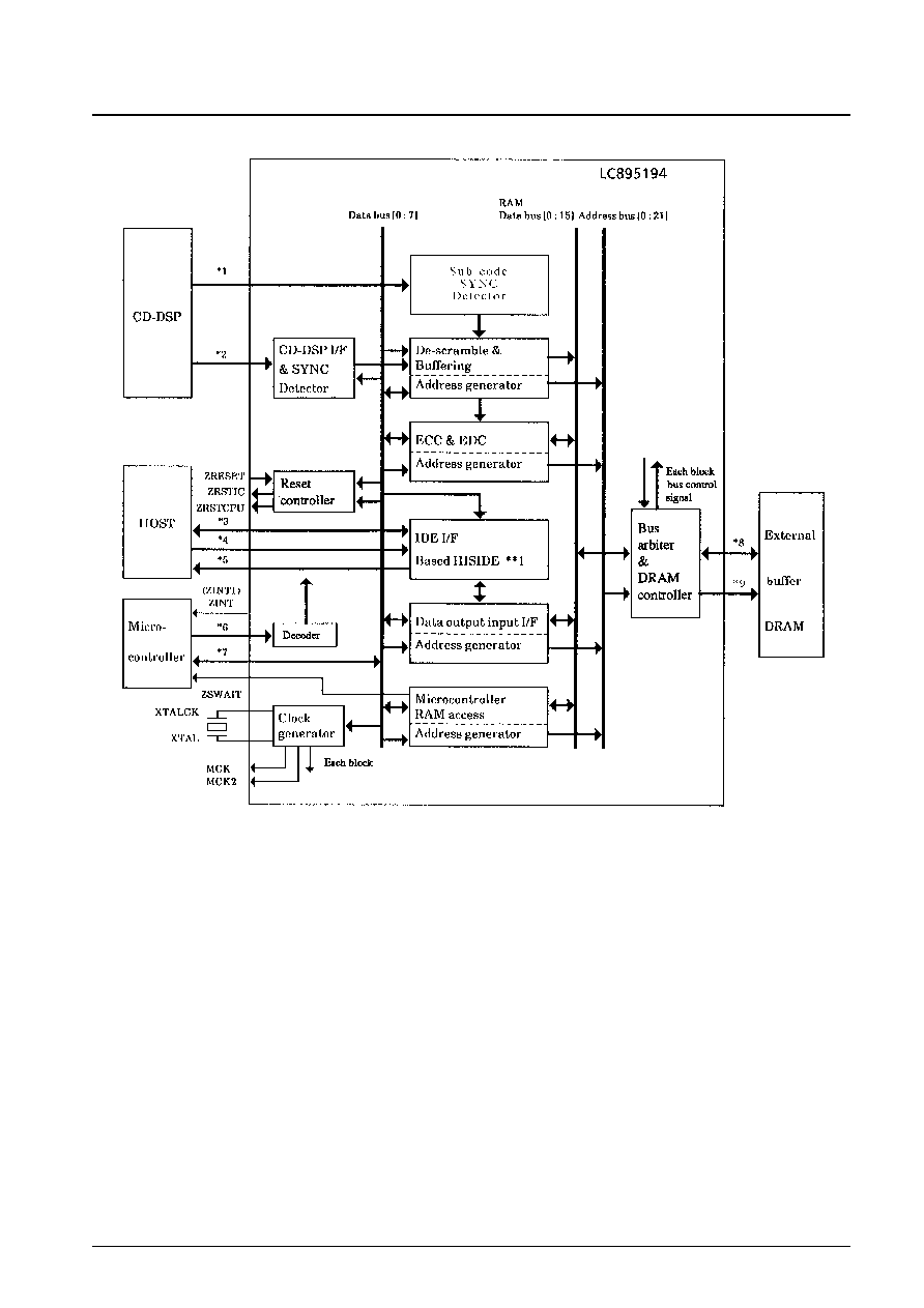
Block Diagram
Note: 1. WFCK, SCOR
2. BCK, SDATA, LRCK, C2PO
3. DD0 to DD15, ZDASP, ZPDIAG
4. ZCS1FX, ZCS3FX, DA0 to DA2, ZDIOR, ZDIOW, ZDMACK
5. DMARQ, HINTRQ, ZIOCS16, IORDY, ZHRST
6. ZRD, ZWR, SUA0 to SUA6, ZCS, CSCTRL
7. D0 to D7
8. IO0 to IO15
9. RA0 to RA9, ZRAS0, ZRAS1, ZCAS0, ZCAS1, ZOE, ZUWE, ZLWE
Note: HISIDE (WD25C32) is made by WESTERN DIGITAL.
No. 5154-3/7
LC895194
Each block
register
R0 to R99
Pin Functions
Type: I: Input pin, O: Output pin, B: Bidirectional pin, P: Power supply pin, NC: No connection pin
Note: 1. NC (no connection) pins must be left open.
2. Pin names (signal names) that begin with a Z have negative (inverted) logic.
3. V
SS0
is the logic system ground and V
SS1
is the IDE interface driver ground.
No. 5154-4/7
LC895194
Pin No.
Symbol
Type
Function
1
V
SS
0
P
2
ZRAS0
O
Buffer DRAM RAS signal output 0 (This pin is used normally.)
3
ZRAS1
O
Buffer DRAM RAS signal output 1
4
V
SS
0
P
5
ZCAS0
O
Buffer DRAM CAS signal output 0 (This pin is used normally.)
6
ZCAS1
O
Buffer DRAM CAS signal output 1
7
V
SS
0
P
8
ZOE
O
Buffer RAM output enable
9
ZUWE
O
Buffer RAM upper write enable
10
ZLWE
O
Buffer RAM lower write enable
11
RA0
O
12
RA1
O
13
RA2
O
14
RA3
O
RA0 to RA9 are the data buffer DRAM address lines.
15
RA4
O
16
RA5
O
17
RA6
O
18
V
DD
P
19
V
SS
0
P
20
RA7
O
21
RA8
O
RA0 to RA9 are the data buffer DRAM address lines.
22
RA9
O
23
NC
24
NC
25
TEST0
NC
26
TEST1
NC
Test pins.
27
TEST2
NC
28
TEST3
NC
29
NC
30
IO0
B
31
IO1
B
32
IO2
B
Data buffer RAM data I/O
33
IO3
B
These pins have built-in pull-up resistors.
34
IO4
B
35
IO5
B
36
V
SS
0
P
37
V
DD
P
38
IO6
B
39
IO7
B
40
IO8
B
41
IO9
B
42
IO10
B
Data buffer RAM data I/O
43
IO11
B
These pins have built-in pull-up resistors.
44
IO12
B
45
IO13
B
46
IO14
B
47
IO15
B
48
EXCK
O
49
WFCK
I
SUB-CODE input/out pin
50
SBSO
I
51
SCOR
I
Continued on next page.
Continued from preceding page.
Type: I: Input pin, O: Output pin, B: Bidirectional pin, P: Power supply pin, NC: No connection pin
Note: 1. NC (no connection) pins must be left open.
2. Pin names (signal names) that begin with a Z have negative (inverted) logic.
3. V
SS0
is the logic system ground and V
SS1
is the IDE interface driver ground.
No. 5154-5/7
LC895194
Pin No.
Symbol
Type
Function
52
V
SS
0
P
53
V
SS
0
P
54
TEST4
I
Test input. This pin must be tied low.
55
V
SS
0
P
56
V
SS
0
P
57
ZINT1
O
Interrupt request signal output to the microcontroller from the IDE block
58
V
SS
0
P
59
V
SS
0
P
60
V
SS
0
P
61
NC
62
NC
63
V
SS
0
P
64
SDATA
I
65
BCK
I
CD-DSP interface
66
LRCK
I
67
C2PO
I
68
MCK2
O
XTALCK 1/1, 1/2, 1/512, and stop output
69
V
SS
0
P
70
XTALCK
I
Crystal oscillator input
71
XTAL
O
Crystal oscillator output
72
V
SS
0
P
73
V
DD
P
74
MCK
O
XTALCK 1/1, 1/2, and stop output
75
V
SS
0
P
76
ZRSTIC
O
Reset signal to drive reset IC
77
CSCTRL
I
Selects active high or active low for the microcontroller CS line.
78
ZRESET
I
LSI reset
79
ZRD
I
Microcontroller data read signal input
80
ZWR
I
Microcontroller data write signal input
81
ZCS
I
Input for the register chip select signal from the microcontroller
82
V
SS
0
P
83
SUA0
I
84
SUA1
I
85
SUA2
I
86
SUA3
I
Microcontroller register select signals
87
SUA4
I
88
SUA5
I
89
SUA6
I
90
V
DD
P
91
V
SS
0
P
92
D0
B
93
D1
B
94
D2
B
95
D3
B
Microcontroller data signals
96
D4
B
These pins have built-in pull-up resistors.
97
D5
B
98
D6
B
99
D7
B
100
ZINT
O
Interrupt request signal output to the microcontroller
Continued on next page.
Continued from preceding page.
Type: I: Input pin, O: Output pin, B: Bidirectional pin, P: Power supply pin, NC: No connection pin
Note: 1. NC (no connection) pins must be left open.
2. Pin names (signal names) that begin with a Z have negative (inverted) logic.
3. V
SS
0 is the logic system ground and V
SS
1 is the IDE interface driver ground.
No. 5154-6/7
LC895194
Pin No.
Symbol
Type
Function
101
ZRSTCPU
O
Reset signal to CPU
102
ZSWAIT
O
Wait signal output to the microcontroller
103
ZHRST
I
104
ZDASP
B
105
ZCS3FX
I
ATAPI control signals
106
ZCS1FX
I
107
DA2
I
108
V
SS
0
P
109
V
DD
P
110
DA0
I
111
ZPDIAG
B
112
DA1
I
ATAPI control signals
113
ZIOCS16
O
114
HINTRQ
O
115
ZDMACK
I
116
V
SS
1
P
117
IORDY
O
118
ZDIOR
I
ATAPI control signals
119
ZDIOW
I
120
DMARQ
O
121
DD15
B
ATAPI data bus
122
V
SS
1
P
123
DD0
B
124
DD14
B
ATAPI data bus
125
DD1
B
126
DD13
B
127
V
SS
1
P
128
V
DD
P
129
DD2
B
130
DD12
B
ATAPI data bus
131
DD3
B
132
V
SS
1
P
133
DD11
B
134
DD4
B
ATAPI data bus
135
DD10
B
136
V
SS
1
P
137
V
DD
P
138
DD5
B
139
DD9
B
ATAPI data bus
140
DD6
B
141
V
SS
1
P
142
DD8
B
ATAPI data bus
143
DD7
B
144
V
DD
P

No. 5154-7/7
LC895194
This catalog provides information as of November, 1997. Specifications and information herein are subject to
change without notice.
s
No products described or contained herein are intended for use in surgical implants, life-support systems, aerospace
equipment, nuclear power control systems, vehicles, disaster/crime-prevention equipment and the like, the failure of
which may directly or indirectly cause injury, death or property loss.
s
Anyone purchasing any products described or contained herein for an above-mentioned use shall:
Accept full responsibility and indemnify and defend SANYO ELECTRIC CO., LTD., its affiliates, subsidiaries and
distributors and all their officers and employees, jointly and severally, against any and all claims and litigation and all
damages, cost and expenses associated with such use:
Not impose any responsibility for any fault or negligence which may be cited in any such claim or litigation on
SANYO ELECTRIC CO., LTD., its affiliates, subsidiaries and distributors or any of their officers and employees
jointly or severally.
s
Information (including circuit diagrams and circuit parameters) herein is for example only; it is not guaranteed for
volume production. SANYO believes information herein is accurate and reliable, but no guarantees are made or implied
regarding its use or any infringements of intellectual property rights or other rights of third parties.