 | –≠–ª–µ–∫—Ç—Ä–æ–Ω–Ω—ã–π –∫–æ–º–ø–æ–Ω–µ–Ω—Ç: LC895199K | –°–∫–∞—á–∞—Ç—å:  PDF PDF  ZIP ZIP |
Ordering number : ENN6238
21000TH (OT)/30899TH (OT) No. 6238-1/12
Overview
The LC895199K is a CD-ROM decoder IC that provides
subcode read functions and an ATAPI interface integrated
on the same chip.
Functions
∑ CD-ROM ECC function
∑ Subcode read function
∑ ATA-PI (IDE) I/F (register block, etc.)
∑ CAV audio function
Features
∑ Built-in ATAPI (IDE) I/F
∑ 32
◊
speed supported:
Using EDO-DRAM (
◊
16, 50 ns)
16.6 Mbytes/s (with IORDY)
Operating frequency: 33.8688 MHz
∑ 32
◊
speed supported:
Using EDO-DRAM (
◊1
6, 45 ns)
16.6 Mbytes/s (without IORDY)
Operating frequency: 33.8688 MHz
∑ 24
◊
speed supported:
Using EDO-DRAM (
◊
16, 50 ns)
16.6 Mbytes/s (without IORDY)
Operating frequency: 33.8688 MHz
∑ 1 Mbits to 4 Mbits of buffer RAM connectable in case
of DRAM
∑ CD main channel, C2 flag, and subcode areas in buffer
RAM can be freely set by user
∑ Built-in batch transfer function (function for sending CD
main channel, C2 flag, subcode, etc. at one time)
∑ Built-in multi-block transfer function (function for
automatically sending several blocks at one time)
∑ Built-in CAV audio function
∑ Built-in intelligent functions (auto buffering, auto
decoding, CD-R support, etc.)
∑ Built-in subcode P to W buffering function (NO-ECC)
and CD-TEXT support
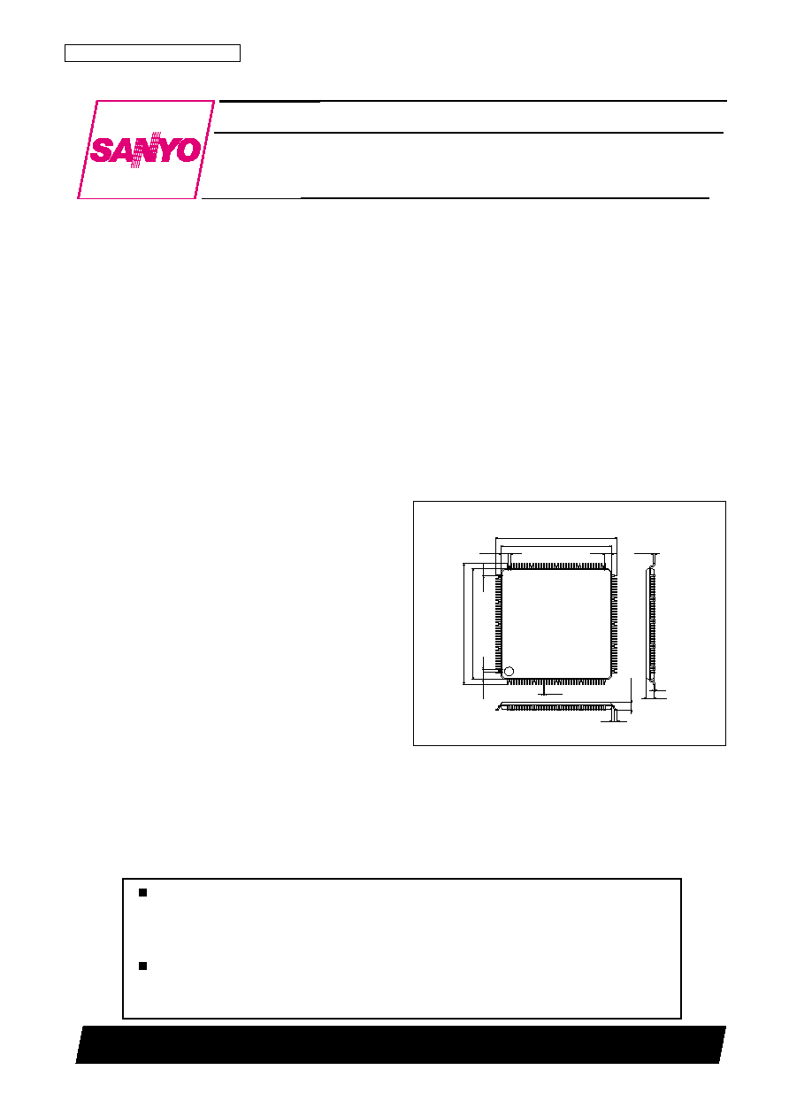
∑ Package: SQFP-144
Package Dimensions
unit: mm
3214-SQFP144
LC895199K
SANYO Electric Co.,Ltd. Semiconductor Company
TOKYO OFFICE Tokyo Bldg., 1-10, 1 Chome, Ueno, Taito-ku, TOKYO, 110-8534 JAPAN
32
◊
CD-ROM Decoder with ATAPI (IDE) Interface
CMOS IC
0.20
1.25
1.25
22.0
20.0
0.5
22.0
20.0
0.5
1.25
1.25
0.145
0.1
1.4
1.6max
0.5
0.5
1
36
37
72
73
108
109
144
SANYO: SQFP144
[LC895199K]
Any and all SANYO products described or contained herein do not have specifications that can handle
applications that require extremely high levels of reliability, such as life-support systems, aircraft's
control systems, or other applications whose failure can be reasonably expected to result in serious
physical and/or material damage. Consult with your SANYO representative nearest you before using
any SANYO products described or contained herein in such applications.
SANYO assumes no responsibility for equipment failures that result from using products at values that
exceed, even momentarily, rated values (such as maximum ratings, operating condition ranges, or other
parameters) listed in products specifications of any and all SANYO products described or contained
herein.
No. 6238-2/12
LC895199K
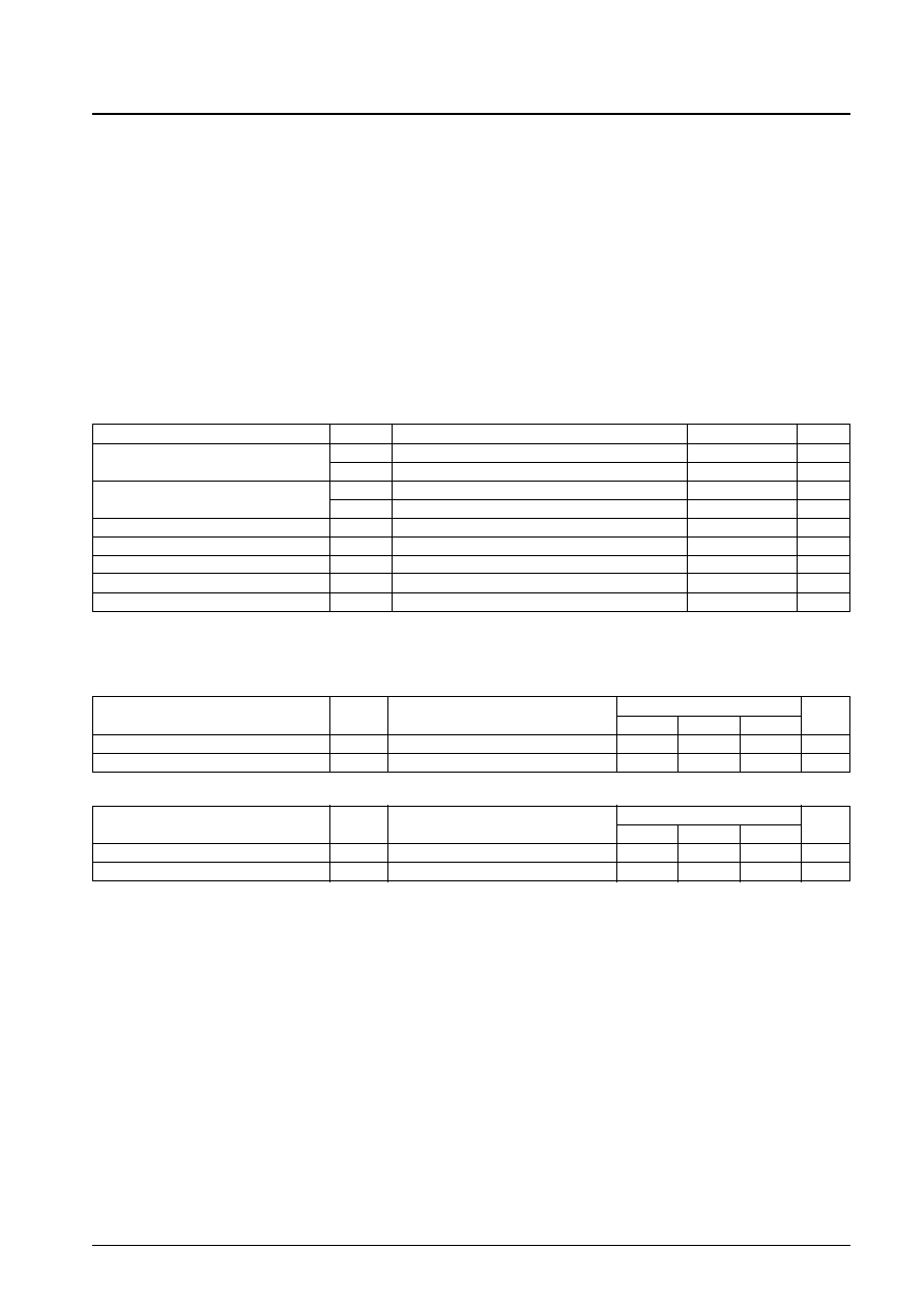
Parameter
Symbol
Conditions
Ratings
Unit
Maximum supply voltage
V
DD
5 max
Ta = 25∞C
≠0.3 to +6.0
V
V
DD
3 max
Ta = 25∞C
≠0.3 to +4.6
V
Input/output voltage
V
I
15, V
O
5
Ta = 25∞C
≠0.3 to V
DD
5 + 0.3
V
V
I
13, V
O
3
Ta = 25∞C
≠0.3 to V
DD
3 + 0.3
V
Allowable power dissipation
Pd max
Ta
70∞C
550
mW
Operating temperature
Topr
≠30 to +70
∞C
Storage temperature
Tstg
≠55 to +125
∞C
Soldering temperature (pin part only)
10 s
235
∞C
Input/output power
I
I
, I
O
*
±20
mA
Specifications
Absolute Maximum Ratings
at V
SS
= 0 V
Note:
*
Per 1 input/output reference cell
Changes from the LC895199
Items changed from the LC895199-MK2
∑ Revision 4.
∑ The DVD-ROM and DVD-RAM interface functions
have been removed.
∑ The buffer circuits for the DRAM pins (RAS, CAS0,
CAS1, OE, WE, and A0 to A8) have been changed from
8 mA sink to 4 mA sink.
∑ The buffer circuits for the D/A converter output pins
(DSDATA, DLRCK, DBCK) have been changed from
8 mA sink to 4 mA sink.
∑ The amount of external DRAM supported has been
changed from 16M to 4M.
∑ The MCK3 output has been changed to a 1/1, 1/2, stop
output.
∑ Settings have been added for cases when the PLL circuit
is not used. (W register R46 bit 7 (set to 1) and C
register R1 (set to 40h))
Parameter
Symbol
Conditions
Ratings
Unit
min
typ
max
Supply voltage
V
DD
3.0
3.3
3.6
V
Input voltage range
V
IN
0
V
DD
V
Internal Cell 3.3 V Supply Voltage
Allowable Operating Range
at Ta = ≠30 to +70∞C, V
SS
= 0 V
Parameter
Symbol
Conditions
Ratings
Unit
min
typ
max
Supply voltage
V
DD
4.5
5.0
5.5
V
Input voltage range
V
IN
0
V
DD
V
I
O
Cell 5.0 V Supply Voltage
No. 6238-3/12
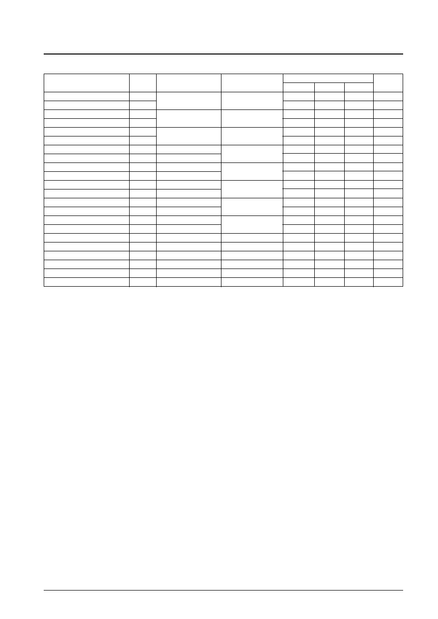
LC895199K
Parameter
Symbol
Conditions
Applicable pins
*
1
Ratings
Unit
min
typ
max
Input high-level voltage
V
IH
TTL levels
(1)
2.2
--
--
V
Input low-level voltage
V
IL
--
--
0.8
V
Input high-level voltage
V
IH
TTL levels
(10)
2.2
--
--
V
Input low-level voltage
V
IL
with pull-down resistor
--
--
0.8
V
Input high-level voltage
V
IH
TTL levels
(2), (3), (11)
2.4
--
--
V
Input low-level voltage
V
IL
Schmitt
--
--
0.8
V
Output high-level voltage
V
OH
I
OH1
= ≠4 mA
(4)
V
DD
≠ 2.1
--
--
V
Output low-level voltage
V
OL
I
OL1
= 4 mA
--
--
0.4
V
Output high-level voltage
V
OH
I
OH1
= ≠8 mA
(10), (12)
V
DD
≠ 2.1
--
--
V
Output low-level voltage
V
OL
I
OL1
= 8 mA
--
--
0.4
V
Output high-level voltage
V
OH
I
OH1
= ≠12 mA
(5)
V
DD
≠ 2.1
--
--
V
Output low-level voltage
V
OL
I
OL1
= 12 mA
--
--
0.4
V
Output high-level voltage
V
OH
I
OH1
= ≠12 mA
(5)
V
DD
≠ 2.1
--
--
V
Output low-level voltage
V
OL
I
OL1
= 12 mA
--
--
0.4
V
Output high-level voltage
V
OH
I
OH1
= ≠4 mA
(8), (11)
V
DD
≠ 2.1
--
--
V
Output low-level voltage
V
OL
I
OL1
= 24 mA
--
--
0.4
V
Output low-level voltage
V
OL
I
OL1
= 24 mA
(9)
--
--
0.4
V
Output low-level voltage
V
OL
I
OL1
= 8 mA
(6), (7)
--
--
0.4
V
Input leakage current
I
IL
V
I
= V
SS
, V
DD
(1), (2), (3), (11)
≠10
+10
µA
Output leakage current
I
OZ
During high-impedance output
(6), (8), (9), (11)
≠10
+10
µA
Pull-up resistance
R
UP
(10)
40
80
160
k
Pull-up resistance
R
UP
ZDMACK *
2
(7)
20
40
80
k
DC Characteristics
at Ta = ≠30 to +70∞C, V
SS
= 0 V, V
DD
= 4.5 to 5.5 V
Notes:1. The applicable pin sets are as follows.
2. When ZDMACK is reset, internal pull-up resistor is OFF.
When Config-Reg-R46 (PULON)-bit 0 (ZDMACK) = 1, pull-up resistor becomes ON.
INPUT
(1)
ATPINSEL, CSCTRL, SUA0 to SUA6, BCK, C2PO, LRCK, SDATA, SBS0, SCOR, WFCK, TEST0 to TEST1
(2)
ZRESET, ZCS, ZRD, ZWR, CSEL
(3)
DA0 to DA2, ZCS1FX, ZCS3FX, ZDIOR, ZDIOW, ZDMACK, ZHRST
OUTPUT
(4)
RA0 to RA8, ZRAS0, ZCAS0 to ZCAS1, ZUWE, ZLWE, ZOE
(5)
MCK, MCK3
(6)
ZRSTCPU
(7)
ZINT, ZINT1, ZSWAIT
(8)
DMARQ, HINTRQ
(9)
IORDY, ZIOCS16
INOUT
(10) D0 to D7, IO0 to IO15, HDB0 to HDB7
(11) DD0 to DD15, ZDASP, ZPDIAG
(12) EXCK
Note: Pins XTAL and XTALCK are not included in the DC characteristics.
No. 6238-4/12
LC895199K
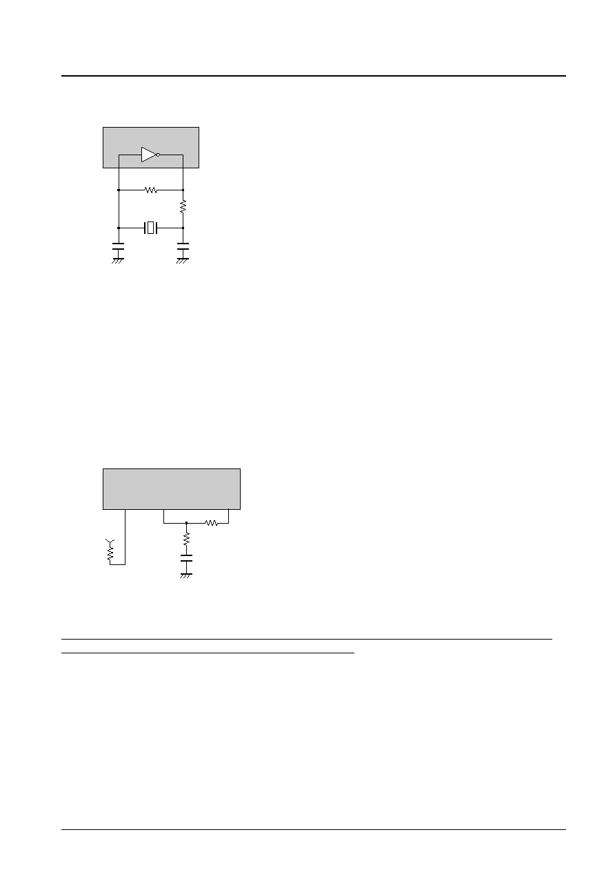
Recommended Oscillator Circuit
LC895199K
R1
R2
C2
C1
XTALCK
PN52
XTAL
PN53
A12521
R1 = 1 M
R2 = 47
C1 = 0
C2 = 47 pF
Ceramic oscillator frequency = 33.8688 MHz.
The 33.8688 MHz frequency in the recommended circuit is the third harmonic.
Since the exact values of these components will vary depending on characteristics of the printed circuit board used and
other factors, consult the manufacturer of the oscillator element when designing the oscillator circuit.
External Circuits for the On-Chip PLL Version (LC895199)
PN69
PN70
PN71
LC895199K
PLL
R5
Analog VSS
R4
C3
R3
3.3V
A12522
R3 = 5.1 k
, R4 = 200
, R5 = 10 k
, C3 = 0.1 µF
The analog V
DD
and V
SS
must be made completely independent of the logic system power supply. In particular, they
must not be affected by fluctuations in the logic system power supply.
No. 6238-5/12
LC895199K
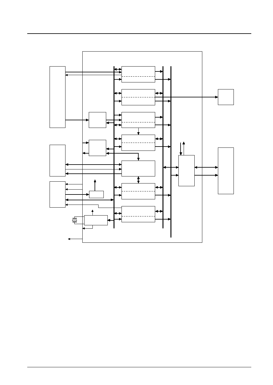
Block Diagram
Sub-code I/F
10byte FIFO for Sub Q
Address generator
Address generator
DAC
CAV-Audio contorol
De-scramble &
Buffering
Address generator
Microcontroller
RAM access
Address generator
Address generator
ECC & EDC
Based HISIDE
IDE I/F
Address generator
Data output input I/F
Bus
Arbiter
&
DRAM
controller
External
Buffer
DRAM
Each Block
Bus control
signal
Each Block
Register
R0-R127
CD-DSP I/F
& SYNC
Detector
Reset
Controller
CD-DSP
HOST
Micro
controller
decoder
Clock generator
& PLL
*1
*2
*8
*10
*9
*6
*7
*11
*3
*5
*4
EXCK
ZRESET
ZINT0
ZINT1
ZSWAIT
ZRSTCPU
XTALCK
XTAL
MCK3
MCK
Each Block
Data bus[0:7]
Address bus[0:17]
RAM
Data bus[0:15]
LC895199K
**1
A12523
*
1
WFCK, SBSO, SCOR
*
2
BCK, SDATA, LRCK, C2PO
*
3
DD0 to DD15, ZDASP, ZPDIAG
*
4
ZCS1FX, ZCS3FX, DA0 to DA2, ZDIOR, ZDIOW, ZDMACK, CSEL
*
5
DMARQ, HINTRQ, ZIOCS16, IORDY, ZHRST
*
6
ZRD, ZWR, SUA0 to SUA6, ZCS, CSCTRL
*
7
D0 to D7
*
8
IO0 to IO15
*
9
RA0 to RA8, ZRAS0, ZCAS0, ZCAS1, ZOE, ZUWE, ZLWE
*
10 DBCK, DLRCK, DSDATA
*
11 IOP0 to IOP7
**
1 HISIDE(WD25C32) is made by WESTERN DIGITAL