 | –≠–ª–µ–∫—Ç—Ä–æ–Ω–Ω—ã–π –∫–æ–º–ø–æ–Ω–µ–Ω—Ç: LC89610 | –°–∫–∞—á–∞—Ç—å:  PDF PDF  ZIP ZIP |
CMOS LSI
Ordering number : EN
*
5120
81095HA (OT) No. 5120-1/7
Preliminary
SANYO Electric Co.,Ltd. Semiconductor Bussiness Headquarters
TOKYO OFFICE Tokyo Bldg., 1-10, 1 Chome, Ueno, Taito-ku, TOKYO, 110-8534 JAPAN
Mini-Disk Decoder LSI
LC89610
Overview
The LC89610 is a playback signal processing CMOS LSI
that supports the mini-disk data format. Data that has been
decoded by a CD decoder, an ACIRC decoder, or a CD-
ROM decoder circuit is passed to a DRAM controller
circuit and the LC89610 uses external DRAM to process
shock proof. The shock proof processed data is passed to
an audio data decoding LSI, the LC89602.
Features
∑ EFM decoder and PLL clock generator
∑ Detection, protection, and interpolation of the EFM
frame synchronization signal
∑ Servo command control
∑ On-chip ACIRC decoder and ACIRC RAM
∑ ±8 frame jitter margin
∑ Powerful error detection and correction (C1: dual errors,
C2: quadruple errors)
∑ CLV control using EFM and ADIP signals
∑ Subcode Q decoding and CRC error checking
∑ Shock proof memory using 1, 4, 16, or 64 Mbits of
external DRAM
∑ Buffering control and management for TOC and UTOC
data
∑ Buffering control and management for subdata
∑ ADIP decoding and CRC error checking
∑ Low-power design using a 0.8 µm rule CMOS process
∑ Support for low-voltage operation (V
DD
= 3.0 to 5.5 V)
∑ CCB based CPU interface
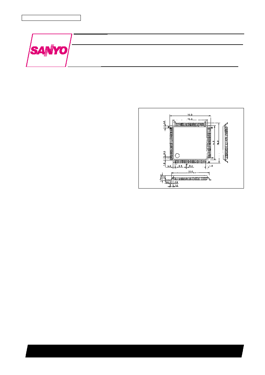
Package Dimensions
unit: mm
3181A-SQFP100
[LC89610]
SANYO: SQFP100
Specifications
Absolute Maximum Ratings
at V
SS
= 0 V
Allowable Operating Ranges
at Ta = ≠30 to +70∞C, V
SS
= 0 V
DC Characteristics
at Ta = ≠30 to +70∞C, V
SS
= 0 V, V
DD
= 4.5 to 5.5 V
Note: 1. HFL, TES, CE, CL, SUBREQ, SREQ, RESET, ADIPCRI, BIDATAI, BICLKI
2. Inputs other than
*
1, 2, and 4 XIN.
3. EFMIN
4. PDO
5. EFMO
6. Outputs other than
*
5 and
*
6 XOUT, AO, and DO (open-drain output).
7. Outputs other than
*
5 and
*
6 XOUT, and AO.
8. For MD0 to MD3, TEST1 to TEST5. However, note that the pull-up resistors are not connected when the PULLSW pin is low.
9. When the PULLSW pin is low, outputs are open, and V
I
= V
SS
or V
DD
.
10.When the PULLSW pin is high, outputs are open, and V
I
= V
SS
or V
DD
.
No. 5120-2/7
LC89610
Parameter
Symbol
Conditions
Ratings
Unit
Maximum supply voltage
V
DD
max
Ta = 25∞C
≠0.3 to +7.0
V
Input and output voltages
V
I
V
O
Ta = 25∞C
≠0.3 to V
DD
+ 0.3
V
Operating temperature
Topr
≠30 to +70
∞C
Storage temperature
Tstg
≠55 to +125
∞C
Soldering conditions
10 seconds (pins only)
260
∞C
Parameter
Symbol
Conditions
min
typ
max
Unit
Supply voltage
V
DD
3.0
5.5
V
Input voltage
V
IN
0
V
DD
V
Parameter
Symbol
Conditions
min
typ
max
Unit
Input high level voltage
V
IH
*
1
0.8 V
DD
V
Input low level voltage
V
IL
*
1
0.2 V
DD
V
Input high level voltage
V
IH
*
2
0.7 V
DD
V
Input low level voltage
V
IL
*
2
0.3 V
DD
V
Input high level voltage
V
IH
*
3
0.6 V
DD
V
Input low level voltage
V
IL
*
3
0.4 V
DD
V
Output high level voltage
V
OH
I
OH
= ≠1 mA,
*
4
V
DD
≠ 0.1
V
Output low level voltage
V
OL
I
OL
= 1 mA,
*
4
0.1
V
Output high level voltage
V
OH
I
OH
= ≠1 mA,
*
5
V
DD
≠ 1.0
V
Output low level voltage
V
OL
I
OL
= 1 mA,
*
5
1.0
V
Output high level voltage
V
OH
I
OH
= ≠3 mA,
*
6
V
DD
≠ 2.1
V
Output low level voltage
V
OL
I
OL
= 3 mA,
*
7
0.4
V
Input leakage current
I
L
V
I
= V
SS
, V
DD
≠10
+10
µA
Output leakage current
I
OZ
For high-impedance state outputs
≠10
+10
µA
Pull-up resistance
R
UP
*
8
10
20
40
k
Quiescent current
I
DD
*
9
0.1
200
µA
Quiescent current
I
DD
*
10
250
475
µA
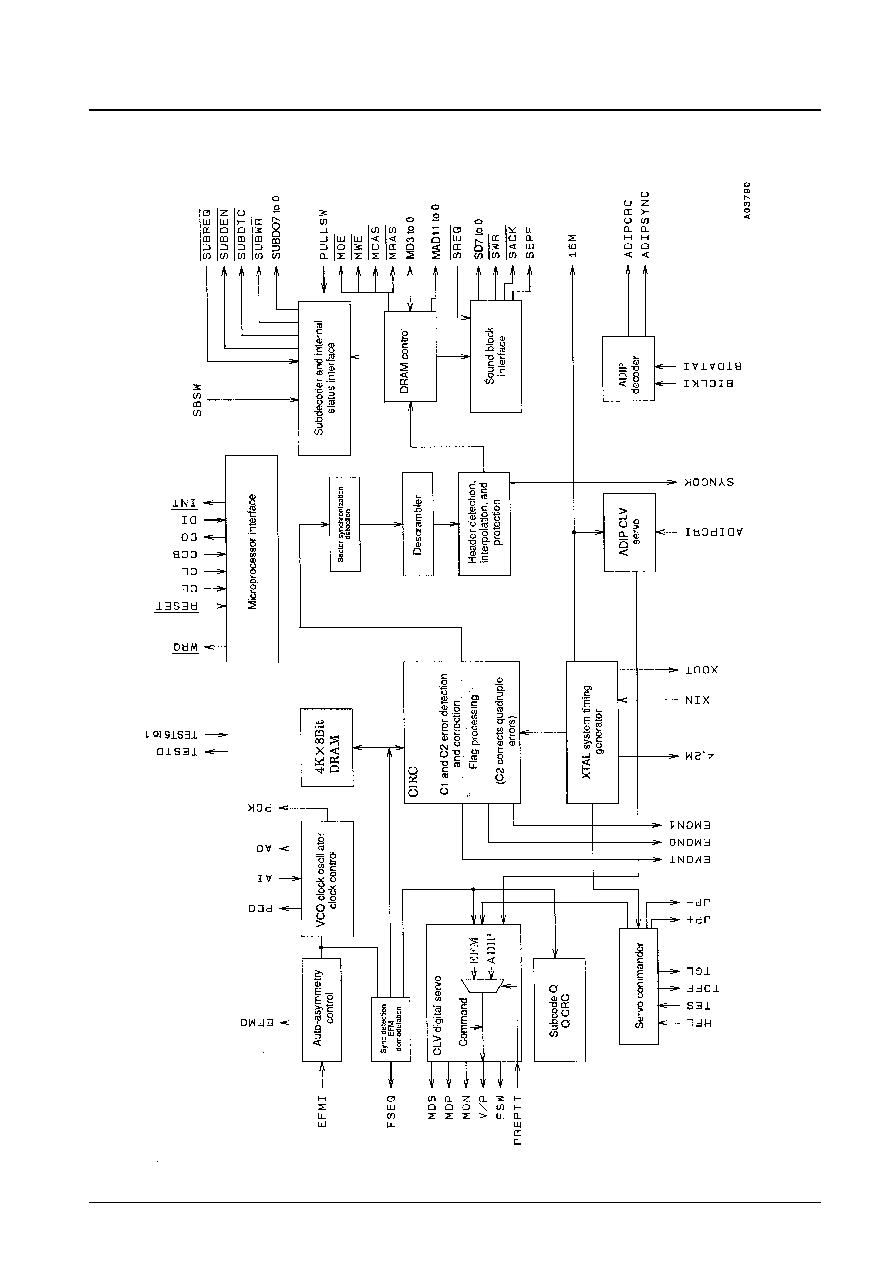
Block Diagram
No. 5120-3/7
LC89610
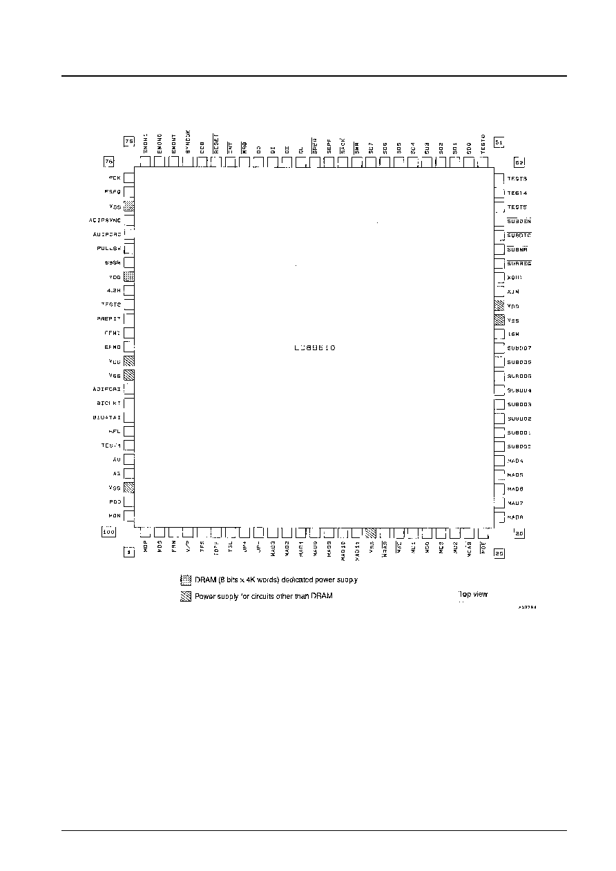
Pin Assignment
No. 5120-4/7
LC89610
Pin Functions
No. 5120-5/7
LC89610
Pin No.
Symbol
I/O
Function
1
MDP
O
CLV servo signal output
2
MDS
O
CLV servo signal output
3
FSW
O
CLV servo signal output
4
V/P
O
CLV servo signal output
5
TES
I
Track jump signal input
6
TOFF
O
Track jump signal output
7
TGL
O
Track jump signal output
8
JP +
O
Track jump signal output
9
JP ≠
O
Track jump signal output
10
MAD3
O
DRAM address output
11
MAD2
O
DRAM address output
12
MAD1
O
DRAM address output
13
MAD0
O
DRAM address output
14
MAD9
O
DRAM address output
15
MAD10
O
DRAM address output
16
MAD11
O
DRAM address output
17
V
SS
--
Ground
18
MRAS
O
DRAM RAS signal output
19
MWE
O
DRAM WE signal output
20
MD1
I/O
DRAM data I/O
21
MD0
I/O
DRAM data I/O
22
MD3
I/O
DRAM data I/O
23
MD2
I/O
DRAM data I/O
24
MCAS
O
DRAM CAS signal output
25
MOE
O
DRAM OE signal output
26
MAD8
O
DRAM address output
27
MAD7
O
DRAM address output
28
MAD6
O
DRAM address output
29
MAD5
O
DRAM address output
30
MAD4
O
DRAM address output
31
SUBDO0
O
Subdata and internal status output
32
SUBDO1
O
Subdata and internal status output
33
SUBDO2
O
Subdata and internal status output
34
SUBDO3
O
Subdata and internal status output
35
SUBDO4
O
Subdata and internal status output
36
SUBDO5
O
Subdata and internal status output
37
SUBDO6
O
Subdata and internal status output
38
SUBDO7
O
Subdata and internal status output
39
16M
O
16.9344 MHz clock output
40
V
SS
--
V
SS
ground
41
V
DD
--
Power supply
42
XIN
I
16.9344 oscillator input
43
XOUT
O
16.9344 oscillator output
44
SUBREQ
I
Subdata request signal input
45
SUBWR
O
Subdata transfer clock output
46
SUBDTC
O
Subdata transfer complete signal output
47
SUBDEN
O
Subdata enable output
48
TEST5
I
Test input (normally tied to V
DD
)
49
TEST4
I
Test input (normally tied to V
DD
)
50
TEST3
I
Test input (normally tied to V
DD
)
51
TESTO
I
Test output
52
SD0
O
Sound block data output
53
SD1
O
Sound block data output
54
SD2
O
Sound block data output
55
SD3
O
Sound block data output
Continued on next page.