 | –≠–ª–µ–∫—Ç—Ä–æ–Ω–Ω—ã–π –∫–æ–º–ø–æ–Ω–µ–Ω—Ç: LC898093 | –°–∫–∞—á–∞—Ç—å:  PDF PDF  ZIP ZIP |
Ordering number : ENN
*
6495
83100RM (OT) No. 6495-1/14
Functions
∑ CD-ROM decoder/encoder functions
∑ CD decoder/encoder functions
∑ Pit and wobble CLV servo
∑ CAV audio functions
∑ ATAPI interface (include the register block)
∑ Subcode encoder/decoder functions
∑ ATIP demodulator/ATIP decoder
∑ Write strategy function (CD-R/RW)
Features
∑ ECC and EDC correction/addition (decoding/encoding)
for CD-ROM data.
∑ ECC error correction/addition (decoding/encoding) for
subcode data
∑ Servo control implemented in a digital servo system
(decoding/encoding)
∑ CLV servo control using ATIP data (encoding)
∑ ATIP decoding function and CRC check function
(decoding/encoding)
∑ CIRC code generation and addition and EFM
modulation (encoding)
∑ CAV audio functions
∑ Provides high-precision CD-R/RW write strategy signal
output
∑ Built-in ATAPI interface (with Ultra DMA 33 support)
∑ Supports 40
◊
decoding and 12
◊
encoding.
Clock frequency: 33.8688 MHz
∑ Transfer rates: Up to 16.6 MB/s (when 32
◊
IORDY
used), up to 33 MB/s when Ultra DMA used. These
values apply when 16-bit 45 ns EDO DRAM is used.
∑ From 1 to 64 Mbits of buffer RAM can be used. (16-bit
data bus EDO DRAM)
∑ The user can freely set up the CD main channel, C2 flag,
and subcode areas in buffer RAM.
∑ Batch transfer function (Function for transferring the CD
main channel, C2 flag, subcode, and other data in a
single operation)
∑ Multi-transfer function (Function for automatically
transferring multiple block to the host in a single
operation)
∑ CAV audio functions
∑ Supports Ultra DMA modes 0, 1, and 2.
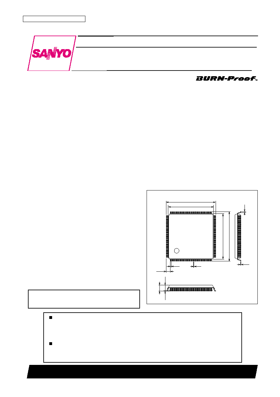
Package Dimensions
unit: mm
3210-SQFP208
28.0
(3.2)
30.6
0.15
0.2
0.35
3.8max
0.5
30.6
(0.5)
(1.25)
28.0
1
52
156
105
53
208
104
157
Preliminary
SANYO: SQFP208
[LC898093]
LC898093
SANYO Electric Co.,Ltd. Semiconductor Company
TOKYO OFFICE Tokyo Bldg., 1-10, 1 Chome, Ueno, Taito-ku, TOKYO, 110-8534 JAPAN
40
◊
Playback/12
◊
Write CD-R/RW Encoder/Decoder IC
with Built-in ATAPI Interface
CMOS IC
Any and all SANYO products described or contained herein do not have specifications that can handle
applications that require extremely high levels of reliability, such as life-support systems, aircraft's
control systems, or other applications whose failure can be reasonably expected to result in serious
physical and/or material damage. Consult with your SANYO representative nearest you before using
any SANYO products described or contained herein in such applications.
SANYO assumes no responsibility for equipment failures that result from using products at values that
exceed, even momentarily, rated values (such as maximum ratings, operating condition ranges, or other
parameters) listed in products specifications of any and all SANYO products described or contained
herein.
"BURN-Proof" stands for Proof against Buffer Under RuN
error, not for proof against burning.
"BURN-Proof" is a trademark of SANYO Electric Co., Ltd.

No. 6495-2/14
LC898093
Parameter
Symbol
Conditions
Ratings
Unit
Supply voltage
V
DD
5 max
Ta
25∞C
≠0.3 to +6.0
V
V
DD
3 max
Ta
25∞C
≠0.3 to +4.6
V
I/O voltages
V
I
5, V
O
5
Ta
25∞C
≠0.3 to V
DD
5 + 0.3
V
V
I
3, V
O
3
Ta
25∞C
≠0.3 to V
DD
3 + 0.3
V
Allowable power dissipation
Pd max
Ta
70∞C
750
mW
Operating temperature
Topr
≠30 to +70
∞C
Storage temperature
Tstg
≠55 to +125
∞C
Soldering conditions (pins only)
10 seconds
260
∞C
Specifications
Absolute Maximum Ratings
at V
SS
= 0 V
Parameter
Symbol
Conditions
Ratings
Unit
min
typ
max
[I/O cells, 5.0 V power supply]
Supply voltage
V
DD
5
4.5
5.0
5.5
V
Input voltage range
V
IN
0
V
DD
5
V
[Internal cells, 3.3 V power supply]
Supply voltage
V
DD
3
3.0
3.3
3.6
V
Input voltage range
V
IN
0
V
DD
3
V
Allowable Operating Ranges
at Ta = ≠30 to +70∞C, V
SS
= 0 V
Parameter
Symbol
Conditions
Ratings
Unit
min
typ
max
High-level input voltage
V
IH
TTL level inputs: (1)
2.2
V
Low-level input voltage
V
IL
0.8
V
High-level input voltage
V
IH
TTL level inputs with built-in pull-up resistors: (4)
2.2
V
Low-level input voltage
V
IL
0.8
V
High-level input voltage
V
IH
TTL level Schmitt trigger inputs: (0), (7)
2.4
V
Low-level input voltage
V
IL
0.8
V
High-level input voltage
V
IH
TTL level Schmitt trigger inputs
2.4
V
Low-level input voltage
V
IL
Built-in pull-up resistors: (9), (14)
0.8
V
High-level input voltage
V
IH
CMOS level inputs with built-in pull-up resistors: (10)
0.7 V
DD
V
Low-level input voltage
V
IL
0.3 V
DD
V
Analog input voltage
V
ANI
(11)
1/4 V
DD
3/4 V
DD
V
High-level output voltage
V
OH
I
OH
= ≠8 mA: (3), (8)
V
DD
≠ 2.1
V
Low-level output voltage
V
OL
I
OL
= 8 mA: (3), (8)
0.4
V
High-level output voltage
V
OH
I
OH
= ≠2 mA: (2), (4), (6)
V
DD
≠ 2.1
V
Low-level output voltage
V
OL
I
OL
= 2 mA: (2), (4), (6)
0.4
V
Low-level output voltage
V
OL
I
OL
= 2 mA: (5)
0.4
V
High-level output voltage
V
OH
I
OH
= ≠8 mA: (7), (12), (14), (15)
V
DD
≠ 2.1
V
Low-level output voltage
V
OL
I
OL
= 24 mA: (7), (12), (14), (15)
0.4
V
Input leakage current
I
IL
V
I
= V
SS
, V
DD
: (0), (1), (7), (9)
≠10
+10
µA
Output leakage current
I
OZ
In the high-impedance output state: (2), (7), (8), (12), (13)
≠10
+10
µA
(14), (15)
Pull-up resistance
R
UP
(10)
50
100
200
k
Pull-up resistance
R
UP
(4), (5)
40
80
160
k
Pull-up resistance
R
UP
(9), (13), (14)
7
10
13
k
Pull-up resistance
R
UP
(15)
7
10
13
k
Electrical Characteristics
at Ta = ≠30 to +70∞C, V
SS
= 0 V, V
DD
= 4.5 to 5.5 V
The applicable pin groups are listed on the following page.

Applicable Pins
[INPUT]
(0) ∑ ∑ ∑ ∑ ∑ ∑ CS, RD, WR, WRITE, SUA0 to SUA7, RESET, WOBBLE, CS1FX, CS3FX, DIOR, DIOW, HRST
(9) ∑ ∑ ∑ ∑ ∑ ∑ DMACK
(1) ∑ ∑ ∑ ∑ ∑ ∑ TEST0 to TEST4
(10) ∑ ∑ ∑ ∑ ∑ FG
(11) ∑ ∑ ∑ ∑ ∑ AD0, AD1, RREC, FE, TE, VREF, AD2, TES
[OUTPUT]
(2) ∑ ∑ ∑ ∑ ∑ ∑ PDS1 to PDS3, DSLB
(3) ∑ ∑ ∑ ∑ ∑ ∑ RA0 to RA9, CAS0 and CAS1, RAS0 to RAS2, LWE, UWE, OE, SSP2/1, RAPC, WAPC, H11T0, LDH,
ATEST3/1, WDAT, NWDAT, EFMG, SHOCK, LOCK, EFMO, ATIPSYNC, ACRCNG, PCK2
(6) ∑ ∑ ∑ ∑ ∑ ∑ LDON
(12) ∑ ∑ ∑ ∑ ∑ INTRQ, IOCS16
(13) ∑ ∑ ∑ ∑ ∑ IORDY
(15) ∑ ∑ ∑ ∑ ∑ DMARQ
[INOUT]
(4) ∑ ∑ ∑ ∑ ∑ ∑ D0 to D7, IO0 to IO15
(5) ∑ ∑ ∑ ∑ ∑ ∑ INT0 and INT1, SWAIT
(7) ∑ ∑ ∑ ∑ ∑ ∑ DD0 to DD15
(8) ∑ ∑ ∑ ∑ ∑ ∑ BIDATA, BICLK
(14) ∑ ∑ ∑ ∑ ∑ DASP, PDIAG
Note: The XTAL0 pin is not specified in the DC characteristics.
The pull-up and pull-down resistors on pins (9), (13), (14), and (15) are disabled after a reset.
No. 6495-3/14
LC898093
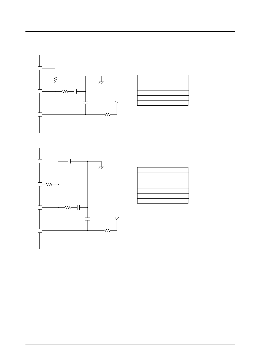
No. 6495-4/14
LC898093
PD
R2
R3
R1
C1
C2
VCNT
R
A13192
PD1
MDC1
R5
R6
R4
C3
C5
C4
VCNT1
R1
A13193
2. Write Strategy Block
The analog V
DD
and V
SS
pins (pins 52, 53, 90, and 91) must be completely isolated from the logic system power supply
and must not be influenced by fluctuations in the logic system power supply.
External Circuit for the PLL Circuit
1. Internal Reference Clock Oscillator Block
Symbol
Value (typ)
Unit
R1
5.6 k
R2
10 k
R3
200
C1
0.1 µ
F
C2
0.1 µ
F
Symbol
Value (typ)
Unit
R4
5.6 k
R5
15 k
R6
220
C3
0.1 µ
F
C4
0.1 µ
F
C5
0.1 µ
F
No. 6495-5/14
LC898093
De-scramble &
Buffering
Address generator
Microcontroller
RAM access
Address generator
Address generator
ECC & EDC
IDE I/F Block
based HISIDE
Address generator
Data output input I/F
Bus
Arbiter
&
DRAM
controller
External
Buffer
DRAM
Each Block
Bus control
signal
Each Block
Register
R0-R255
CD-DSP I/F
& SYNC
Detector
Digital Servo
&
CIRC EnDec
HOST
Micro
controller
decoder
PLL
&
Clock
generator
*8
DAC
*9
*13
*10
*6
*7
*3
*4
*5
CAV-Audio
Sub-code ECC
Address generator
*1
Write Strategy
&
Link-position
*12
Sub-code I/F
de-interleve/interleve
Address generator
*11
ATIP/CLV servo
ATIPSYNC
INT0, INT1
ZSWAIT
XTALCK0
XTAL0
Each Block
Data bus[0:7]
Address bus[0:21]
RAM
Data bus[0:15]
LC898093
A13194
Block Diagram
*1 DSLB (pin96) to SUBSYNC (pin145), SHOCK (pin147) to PCK2 (pin155)
*3 DD0 to DD15, DASP, PDIAG
*4 CS1FX, CS3FX, DA0 to DA2, DIOR, DIOW, DMACK
*5 DMARQ, HINTRQ, IOCS16, IORDY
*6 RD, WR, SUA0 to SUA7, CS
*7 D0 to D7
*8 IO0 to IO15
*9 RA0 to RA9, RAS0, RAS1, RAS2, CAS0, CAS1, OE, UWE, LWE
*10 WOBBLE
*11 ATIPSYNC, BIDATA, BICLK
*12 WRITE, SSP2/1, RAPC, WAPC, H11T0, LDH, ATEST3, ATEST1, WDAT, NWDAT, EFMG
*13 LOUT, ROUT
**1 HISIDE (WD25C32) is made by WESTERN DIGITAL.