 | –≠–ª–µ–∫—Ç—Ä–æ–Ω–Ω—ã–π –∫–æ–º–ø–æ–Ω–µ–Ω—Ç: LC89902V | –°–∫–∞—á–∞—Ç—å:  PDF PDF  ZIP ZIP |

Overview
The LC89902V is a vertical driver CMOS IC specifically
designed for use with VGA-format CCD image sensors.
Applications
∑ Image input units and similar products
Features
∑ CMOS structure supporting low power dissipation.
∑ Level shifter circuits provided on chip to minimize the
number of external components required.
∑ Miniature package (24-pin SSOP)
Functions
∑ Inverting drivers: 6 channels
-- Converts input pulses to V
CC
1, V
CC
2, and V
CC
3, as
well as V
EE
1 and V
EE
2 levels (inverting).
-- Generates the drive levels required for the image
sensor imaging and storage sections.
∑ Inverting drivers: 2 channels
-- These drivers convert input pulses to V
CC
1, V
CC
2,
and V
CC
3, as well as V
EE
1 and V
EE
2 levels
(inverting).
-- These drivers generate the drive levels required for
the image sensor transfer gate.
Package Dimensions
unit: mm
3175A-SSOP24
CMOS LSI
Ordering number : EN5741
93097HA (OT) No. 5741-1/5
SANYO Electric Co.,Ltd. Semiconductor Bussiness Headquarters
TOKYO OFFICE Tokyo Bldg., 1-10, 1 Chome, Ueno, Taito-ku, TOKYO, 110 JAPAN
CMOS Driver for VGA-Format Image Sensors
LC89902V
Specifications
Absolute Maximum Ratings
at Ta = 25∞C
Allowable Operating Ranges
at Ta = 25∞C
[LC89902V]
SANYO: SSOP24
Parameter
Symbol
Condition
Ratings
Unit
Maximum supply voltage
V
CC
max
V
CC
1, V
CC
2, V
CC
3
≠0.3 to +6.0
V
V
EE
max
V
EE
1, V
EE
2
≠11.0 to +0.3
V
Input and voltages
V
IN
All input pins
≠0.3 to V
CC
+ 0.3
V
Allowable power dissipation
Pd max
350
mA
Operating temperature
Topr
≠10 to +70
∞C
Storage temperature
Tstg
≠40 to +125
∞C
Parameter
Symbol
Conditions
Ratings
Unit
Supply voltage
V
CC
V
CC
1, V
CC
2, V
CC
3
4.5 to 5.5
V
V
EE
V
EE
1, V
EE
2
≠10.5 to 0
V
Input voltage range
V
IN
All input pins
0 to V
CC
V
No. 5741-2/5
LC89902V
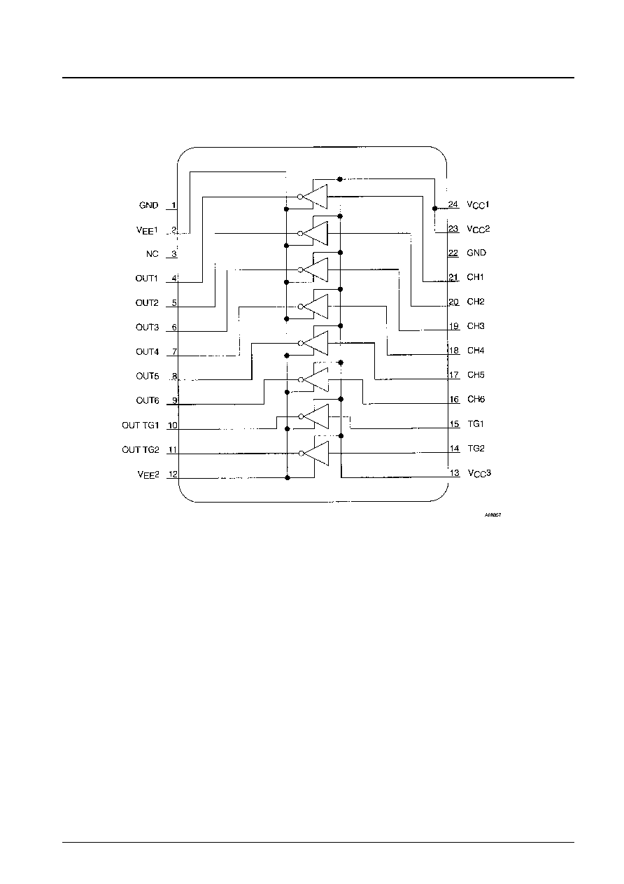
Block Diagram
No. 5741-3/5
LC89902V
Pin Functions
Pin No.
Pin name
Function
1
GND
Ground
2
V
EE
1
Negative power supply used to set the low output level
3
NC
≠
4
OUT1
Channel 1 driver output
5
OUT2
Channel 2 driver output
6
OUT3
Channel 3 driver output
7
OUT4
Channel 4 driver output
8
OUT5
Channel 5 driver output
9
OUT6
Channel 6 driver output
10
OUT TG1 Transfer gate 1 driver output
11
OUT YG2 Transfer gate 2 driver output
12
V
EE
2
Negative power supply used to set the low output level
13
V
CC
3
Positive power supply used to set the high output level
14
TG2
Transfer gate 2 driver input
15
TG1
Transfer gate 1 driver input
16
CH6
Channel 6 driver input
17
CH5
Channel 5 driver input
18
CH4
Channel 4 driver input
19
CH3
Channel 3 driver input
20
CH2
Channel 2 driver input
21
CH1
Channel 1 driver input
22
GND
Ground
23
V
CC
2
Positive power supply used to set the high output level
24
V
CC
1
Positive power supply used to set the high output level
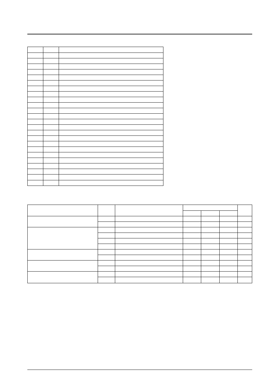
Parameter
Symbol
Conditions
Ratings
Unit
min
typ
max
Input high-level current
I
IH
All input pins, V
IN
= 5.0 V
10
µA
I
IL
All input pins, V
IN
= 0 V
5
nA
I
CCH
+
V
CC
1, V
CC
2, and V
CC
3, all input pins, V
IN
= 5.0 V
1
µA
Supply current
I
CCH
≠
V
EE
1 and V
EE
2, all input pins, V
IN
= 5.0 V
≠10
µA
I
CCL
+
V
CC
1, V
CC
2, and V
CC
3, all input pins, V
IN
= 0 V
7
µA
I
CCL
≠
V
EE
1 and V
EE
2, all input pins, V
IN
= 0 V
≠2
µA
Output voltage
V
OH
All input pins, V
IN
= 0 V
5.0
V
V
OL
All input pins, V
IN
= 5.0 V
≠10
V
Output voltage under actual operating conditions
V
OH
2
Load = LC99152, input = LC99055 *
5.0
V
V
OL
2
Load = LC99152, input = LC99055 *
≠10
V
Output current under actual operating conditions
I
CC
2
+
Load = LC99152, input = LC99055 *
1.62
mA
I
CC
2
≠
Load = LC99152, input = LC99055 *
1.61
mA
Electrical Characteristics
at Ta = 25∞C, V
CC
1, V
CC
2, and V
CC
3 = 5.0 V, V
EE
1 and V
EE
2 = ≠10.0 V
Note:
*
Values for when the LC99055 timing IC provides the input pulses and the LC99152 image sensor is driven. These values are provided for reference
purposes only.
No. 5741-4/5
LC89902V
Switching Characteristics
at Ta = 25∞C, V
CC
1, V
CC
2, and V
CC
3 = 5.0 V, V
EE
1 and V
EE
2 = ≠10.0 V, f
IN
= 3.58 MHz
Note: Load conditions
RL = 18
, CL = 780 pF
Load Circuit
Switching Waveforms
Truth Table
Usage Notes
∑ Power supply application timing
When applying power to the LC89902V, either both power-supply voltages must be turned on at the same time or V
CC
(+5 V) must be turned on before V
EE
(≠10 V) is turned on. The IC may be destroyed if V
EE
is turned on first.
∑ Power supply noise elimination
Clock frequency noise may occur on the power supply lines due to the charge and discharge currents required to drive
the CCD. Capacitors must be inserted both between V
CC
and ground and between V
EE
and ground to eliminate noise
from the power supply lines. These capacitors must have values of at least 47 µF.
Parameter
Symbol
Conditions
Ratings
Unit
min
typ
max
Propagation delay time
t
PLH
All output pins
23
ns
Low level
high level
Propagation delay time
t
PHL
All output pins
31
ns
High level
low level
Rise time
tr
All output pins
47
ns
Fall time
tf
All output pins
42
ns
Output
Input
H
V
OL
L
V
OH
All inputs
All outputs

No. 5741-5/5
LC89902V
This catalog provides information as of September, 1997. Specifications and information herein are subject to
change without notice.
s
No products described or contained herein are intended for use in surgical implants, life-support systems, aerospace
equipment, nuclear power control systems, vehicles, disaster/crime-prevention equipment and the like, the failure of
which may directly or indirectly cause injury, death or property loss.
s
Anyone purchasing any products described or contained herein for an above-mentioned use shall:
Accept full responsibility and indemnify and defend SANYO ELECTRIC CO., LTD., its affiliates, subsidiaries and
distributors and all their officers and employees, jointly and severally, against any and all claims and litigation and all
damages, cost and expenses associated with such use:
Not impose any responsibility for any fault or negligence which may be cited in any such claim or litigation on
SANYO ELECTRIC CO., LTD., its affiliates, subsidiaries and distributors or any of their officers and employees
jointly or severally.
s
Information (including circuit diagrams and circuit parameters) herein is for example only; it is not guaranteed for
volume production. SANYO believes information herein is accurate and reliable, but no guarantees are made or implied
regarding its use or any infringements of intellectual property rights or other rights of third parties.