NTSC CCD 1H Delay Line
Overview
The Sanyo LC8991 is a 1H delay line for NTSC television
systems.
Features
.
Single 9 V power supply
.
Low clock input voltage
.
1H delay signal can be obtained with low-pass filter and
7.16 MHz clock input
.
Minimum number of external components required because
timing generator, driver, bias generator and output amplifier
are built in
.
8-pin DIP (Small package)
Functions
.
453 stages CCD shift register
.
CCD drive circuit
.
Auto-bias circuit
.
Sync tip clamp circuit
.
Sample-and-hold circuit
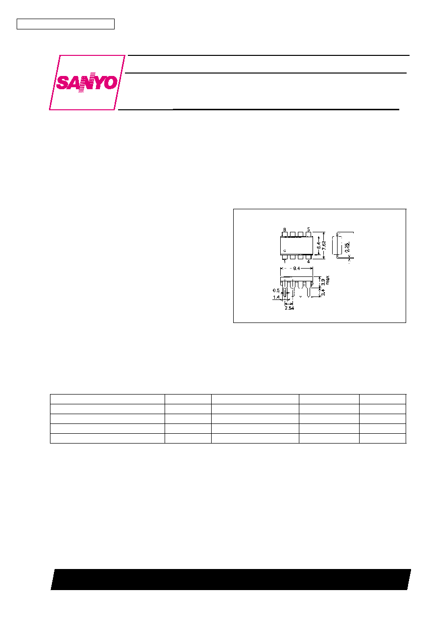
Package Dimensions
unit : mm
3001B-DIP8
[LC8991]
SANYO : DIP8
Specifications
Absolute Maximum Ratings
at Ta = 25�C
Parameter
Symbol
Conditions
Ratings
Unit
Maximum supply voltage
V
DD
max
11
V
Allowable power dissipation
Pd max
500
mW
Operating temperature
Topr
�10 to +60
�C
Storage temperature
Tstg
�55 to +125
�C
Ordering number: EN3202A
LC8991
SANYO Electric Co.,Ltd. Semiconductor Bussiness Headquarters
TOKYO OFFICE Tokyo Bldg., 1-10, 1 Chome, Ueno, Taito-ku, TOKYO, 110 JAPAN
13097HA(II)/N090JN, JK/8290TA No.3202-1/4

Electrical Characteristics
Parameter
Symbol
Conditions
min
typ
max
Unit
DC Characteristics at Ta = 25�C, V
DD
= 9 V, CLOCK = 7.15909 MHz; 0.3 Vp-p
Supply voltage
V
DD
8.5
9.0
9.5
V
Supply current
I
DD
16.5
20.0
mA
DC output voltage
V
GG
13.5
V
OUT
3.1
V
VOB
4.5
V
VID IN
2.8
V
CLK
2.0
V
COMP
2.7
V
AC Characteristics at Ta = 25�C, V
DD
= 9 V, CLOCK = 7.15909 MHz ; 0.3 Vp-p
Maximum input voltage
V
IN
max
0.5
0.7
Vp-p
Voltage gain
VG
Input : 15 kHz, 0.5 Vp-p
6
9
11
dB
Linearity
L6
b/a, Note 1
56
60
64
%
L2
c/a, Note 1
18
20
22
%
LS
d/a, Note 1
37
40
43
%
Frequency response
Gf
Note 2
�3.0
�2.3
dB
Noise
V
NO
3.4 MHz bandwidth
1.1
mVrms
Clock input voltage
Eck
0.1
0.3
1.0
Vp-p
Output impedance
Z
O
520
Delay time
t
O
63.42
�s
Note 1) Linearity test
Input: 5 step staircase signal
Note 2) Frequency response test
Input = 0.5 Vp-p sine wave (2.4 MHz)/(20 kHz)
Pin Assignment
Pin Description
Pin No.
Symbol
Function
1
V
DD
Power supply
2
V
SS
GND
3
V
GG
V
GG
voltage output
4
OUT
Delay signal output
5
VOB
Feedback output
6
VID IN
Signal input
7
CLK
Clock input
8
COMP
Duty cycle compensation output
LC8991
No.3202-2/4
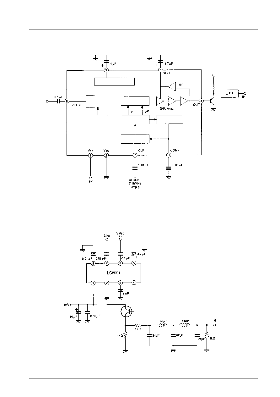
Block Diagram
Sample Application Circuit
V
GG
voltage generator
Sync tip
clamp
Input signal
Auto-bias
circuit
CCD 453 stages
Clock driver
Wave shaper
sine wave
Duty cycle
detector
Delay output signal
V
GG
Delay output
LC8991
No.3202-3/4

No products described or contained herein are intended for use in surgical implants, life-support systems, aerospace equipment,
nuclear power control systems, vehicles, disaster/crime-prevention equipment and the like, the failure of which may directly or
indirectly cause injury, death or property loss.
Anyone purchasing any products described or contained herein for an above-mentioned use shall:
1
Accept full responsibility and indemnify and defend SANYO ELECTRIC CO., LTD., its affiliates, subsidiaries and distributors
and all their officers and employees, jointly and severally, against any and all claims and litigation and all damages, cost and
expenses associated with such use:
2
Not impose any responsibility for any fault or negligence which may be cited in any such claim or litigation on SANYO
ELECTRIC CO., LTD., its affiliates, subsidiaries and distributors or any of their officers and employees jointly or severally.
Information (including circuit diagrams and circuit parameters) herein is for example only; it is not guaranteed for volume
production. SANYO believes information herein is accurate and reliable, but no guarantees are made or implied regarding its use
or any infringements of intellectual property rights or other rights of third parties.
This catalog provides information as of January, 1997. Specifications and information herein are subject to change without notice.
LC8991
No.3202-4/4