 | –≠–ª–µ–∫—Ç—Ä–æ–Ω–Ω—ã–π –∫–æ–º–ø–æ–Ω–µ–Ω—Ç: LC89950 | –°–∫–∞—á–∞—Ç—å:  PDF PDF  ZIP ZIP |
MOS LSI
Ordering number : EN
*
5440
D3097HA(OT) No. 5440-1/5
Preliminary
SANYO Electric Co.,Ltd. Semiconductor Bussiness Headquarters
TOKYO OFFICE Tokyo Bldg., 1-10, 1 Chome, Ueno, Taito-ku, TOKYO, 110 JAPAN
1H Delay Line for PAL Systems
LC89950
Overview
The LC89950 is an IC that provides 1H delay processing
for color difference signals used in PAL and SECAM
format TV. The LC89950 has two CCD systems, one for
the R-Y and one for the B-Y signal, and drives these
CCDs with a 4-MHz clock generated within the IC. It uses
a sandcastle-shaped three-value input clock with a 1 H (64
µs) period.
Features
∑ 5-V single-voltage power supply
∑ Two input and output systems, one each for R-Y and B-
Y signals
∑ Takes a sandcastle pulse (SCP) as the input clock, and
converts that to a burst gate pulse (BGP) signal
internally.
∑ Generates the CCD drive pulses (4 MHz) from the input
clock using a PLL circuit.
∑ Uses BGP as clamp pulses and clamps the no signal
section (back porch) once every horizontal scan period.
∑ The output signal is in-phase with the input signal
Functions
∑ Two on-chip 254.5-bit CCD shift registers
∑ CCD drive circuits
∑ Sample-and-hold circuit
∑ Burst gate pulse detection circuit
∑ 256
◊
PLL circuit
∑ Auto-bias and input clamping circuits
∑ 4-MHz output circuit
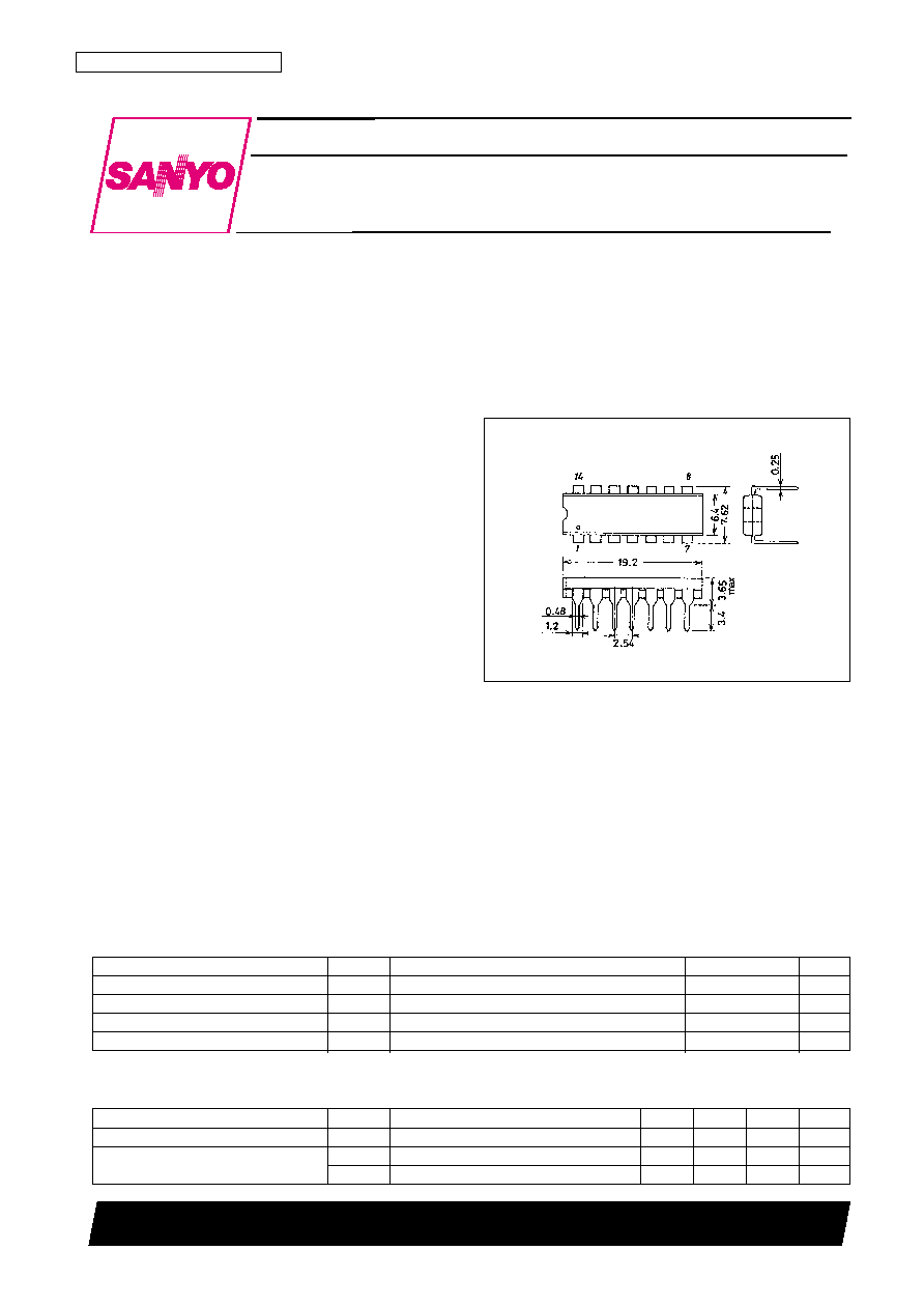
SANYO: DIP14
[LC89950]
Package Dimensions
unit: mm
3003A-DIP14
Parameter
Symbol
Conditions
Ratings
Unit
Supply voltage
V
DD
≠0.3 to +6.0
V
Allowable power dissipation
Pd max
450
mW
Operating temperature
Topr
≠10 to +60
∞C
Storage temperature
Tstg
≠55 to +125
∞C
Specifications
Absolute Maximum Ratings
at Ta = 25∞C
Allowable Operating Ranges
at Ta = 25∞C
Parameter
Symbol
Conditions
min
typ
max
Unit
Supply voltage
V
DD
4.75
5.0
5.25
V
Input signal amplitude
V
INPP(R-Y)
500
700
mV
V
INPP(B-Y)
500
700
mV

No. 5440-2/5
LC89950
Electrical Characteristics
at Ta = 25∞C, V
DD
= 5.0 V, Fscp = 15.625 kHz
Parameter
Symbol
Switch States
min
typ
max
Unit
Test
SW1
SW2
SW3
SW4
conditions
Current drain
I
DD
a/b
a
a/b
a/b
1
5
10
15
mA
Output pin voltage (pin 1)
V
OUT
(R-Y)
b
a
a/b
a/b
2
0.7
1.7
2.7
V
Output pin voltage (pin 3)
V
OUT
(B-Y)
a
a
a/b
a/b
2
0.7
1.7
2.7
V
Input pin voltage (pin 7)
V
IN
(R-Y)
b
a
a/b
a/b
2
1.4
2.4
3.4
V
Input pin voltage (pin 5)
V
IN
(B-Y)
a
a
a/b
a/b
2
1.4
2.4
3.4
V
Voltage gain
G
V
(R-Y)
a
a
a
a
3
≠2
0
+2
dB
G
V
(B-Y)
b
a
a
a
3
≠2
0
+2
dB
Differential voltage gain
G
V
a
b
a
a
a
3
0.1
0.3
dB
Frequency characteristics
G
f
(R-Y)
a
a
a
a
4
≠3
≠1
dB
G
f
(B-Y)
b
a
a
a
4
≠3
≠1
dB
Positive phase input linearity +L6
+L6 (R-Y)
a
a
a
b
5
57
60
63
%
+L6 (B-Y)
b
a
a
b
5
57
60
63
%
Inverted input linearity ≠L6
≠L6 (R-Y)
a
a
b
b
5
57
60
63
%
≠L6 (B-Y)
b
a
b
b
5
57
60
63
%
Clock leakage (4 MHz)
Lclk (R-Y)
a
a
a
a
6
7
12
mVrms
Lclk (B-Y)
b
a
a
a
6
7
12
mVrms
Noise level
No (R-Y)
a
a
a
b
7
1
2
mVrms
No (B-Y)
b
a
a
b
7
1
2
mVrms
Output impedance
Z
OUT
(R-Y)
a
a
b
a
a
8
200
300
400
Z
OUT
(B-Y)
b
a
b
a
a
8
200
300
400
Delay time
Td (R-Y)
a
a
a
a
9
63.80
µs
Td (B-Y)
b
a
a
a
9
63.80
µs
Sandcastle Pulse (Input Clock) Conditions
Notes: 1. Indicates the synchronization range for the PLL circuit. The delay time changes with the input frequency.
2. Vhigh is the minimum value between c and d.
3. Vmid is the maximum value between a and b and between e and f.
Parameter
Symbol
Conditions
min
typ
max
Unit
Input frequency
*
1
Fscp
14.625
15.625
16.625
kHz
Input pulse width
TW bgp
3.0
4.0
5.0
µs
High level
*
2
Vhigh
5.9
6.5
7.5
V
Mid level
*
3
Vmid
2.5
3.5
4.4
V
Low level
Vlow
≠0.3
0
2.5
V

Test Conditions
1. Measure the power-supply current when no input signal is supplied.
2. Measure the pin voltages on each pin when no input signal is supplied.
3. Let V
OUT
be the OUT pin signal amplitude when a 200-kHz 350-mVp-p sine wave is input.
Then, the voltage gain (G
V
) for each of the R-Y and B-Y I/O systems is given by:
V
OUT
[mVp-p]
G
V
= 20log -------------- [dB]
350 [mVp-p]
The R-Y and B-Y voltage gains (
G
V
) are:
G
V
= | G
V
(R-Y) ≠G
V
(B-Y)|
4. Let V1 be the OUT pin output when a 100-kHz 200-mVp-p sine wave is input.
Let V2 be the OUT pin output when a 1-MHz 200-mVp-p sine wave is input.
V2 [mVp-p]
G
f
= 20log -------------- [dB]
V1 [mVp-p]
5. Input a 5-stage step waveform (350 mVp-p) and measure the levels a and b in the output signals.
Perform those measurements for both positive phase and inverted signal inputs.
<Positive phase signal input>
<Inverted signal input>
6. Measure the noise spectrum of the output signal when no input is supplied and read the 4-MHz peak.
7. Pass the output signal through a 2-MHz low-pass filter and a 100-kHz high-pass filter. Then, measure that output with
a noise meter, when no input signal is supplied. Use a 2-MHz low-pass filter with an attenuation of ≠60 dB at 4-MHz.
8. Input a 200-kHz 350-mVp-p sine wave.
Let V1 be the OUT pin output when SW2 is set to a.
Let V2 be the OUT pin output when SW2 is set to b.
V1 [mVp-p] ≠ V2 [mVp-p]
Z
O
= ------------------------
◊
500 [
]
V2 [mVp-p]
9. Measure the delay time of the OUT pin output with respect to the input signal. When taking this measurement, exclude
the delay associated with the low-pass filter.
No. 5440-3/5
LC89950

Pin Assignment
Note: Pins 1 and 3 are referred to collectively as the "OUT pin."
Block Diagram
No. 5440-4/5
LC89950
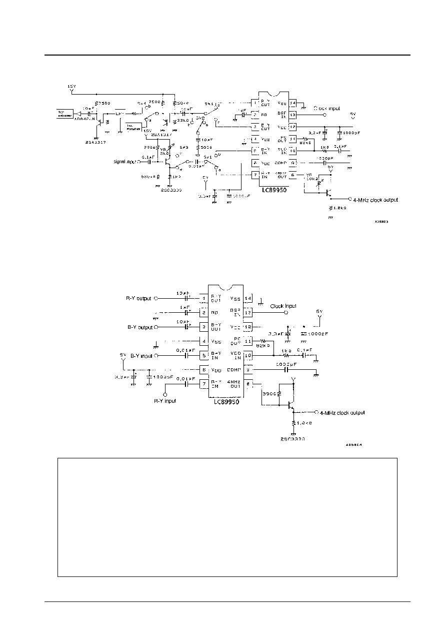
Test Circuit
Notes: 1. Adjust VR (2 k
) so that the output amplitudes when SW3 is set to the a and b positions are equal.
2. LPF is a 2-MHz low-pass filter. Use a filter with an attenuation of ≠60 dB at 4 MHz.
3. The operational amplifier (AD842JN) is a non-inverting amplifier, and the gain from the SW1 output to the operational amplifier output should be 0 dB.
Sample Application Circuit
No. 5440-5/5
LC89950
This catalog provides information as of December, 1997. Specifications and information herein are subject to
change without notice.
s
No products described or contained herein are intended for use in surgical implants, life-support systems, aerospace
equipment, nuclear power control systems, vehicles, disaster/crime-prevention equipment and the like, the failure of
which may directly or indirectly cause injury, death or property loss.
s
Anyone purchasing any products described or contained herein for an above-mentioned use shall:
Accept full responsibility and indemnify and defend SANYO ELECTRIC CO., LTD., its affiliates, subsidiaries and
distributors and all their officers and employees, jointly and severally, against any and all claims and litigation and all
damages, cost and expenses associated with such use:
Not impose any responsibility for any fault or negligence which may be cited in any such claim or litigation on
SANYO ELECTRIC CO., LTD., its affiliates, subsidiaries and distributors or any of their officers and employees
jointly or severally.
s
Information (including circuit diagrams and circuit parameters) herein is for example only; it is not guaranteed for
volume production. SANYO believes information herein is accurate and reliable, but no guarantees are made or implied
regarding its use or any infringements of intellectual property rights or other rights of third parties.