Ordering number : EN
*
5391
41596HA (OT) No. 5391-1/7
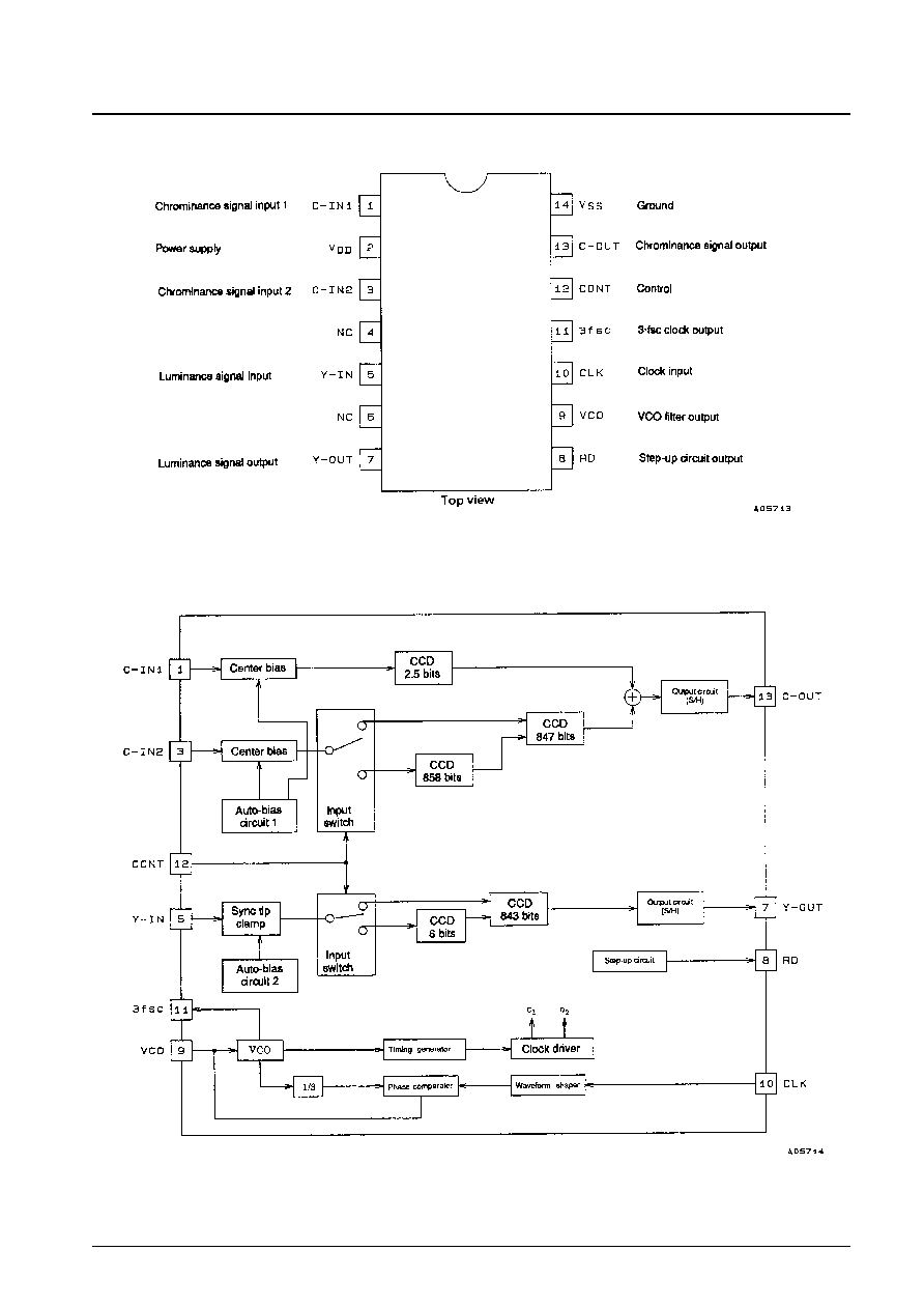
Overview
The LC89975M is a lower-cost PAL-Format CCD delay
line based on the LC89970M, with the sizes of chip and
package miniaturized and the external parts count reduced.
Features
∑ 5 V single-voltage power supply
∑ On-chip 3
◊
PLL circuit for 3∑fsc operation from an fsc
(4.43 MHz) input
∑ Supports PAL/GBI and 4.43 NTSC systems, selected by
a control pin input
∑ Includes an on-chip comb filter for chrominance signal
crosstalk exclusion. This adjustment-free circuit
provides high-precision comb characteristics.
∑ Peripheral circuits included on chip to allow operation
with minimal external circuits.
∑ Positive-phase signal input, positive phase signal output
(luminance signal)
Functions
∑ CCD shift register (for chrominance and luminance
signals)
∑ CCD drive circuit
∑ Circuit for switching the number of CCD stages
∑ CCD signal addition circuit
∑ Auto-bias circuit
∑ Sync tip clamping circuit (luminance signal)
∑ Center bias circuit (chrominance signal)
∑ Sample-and-hold circuit
∑ PLL 3
◊
circuit
∑ 3∑fsc clock output circuit
∑ RD voltage generation step-up circuit
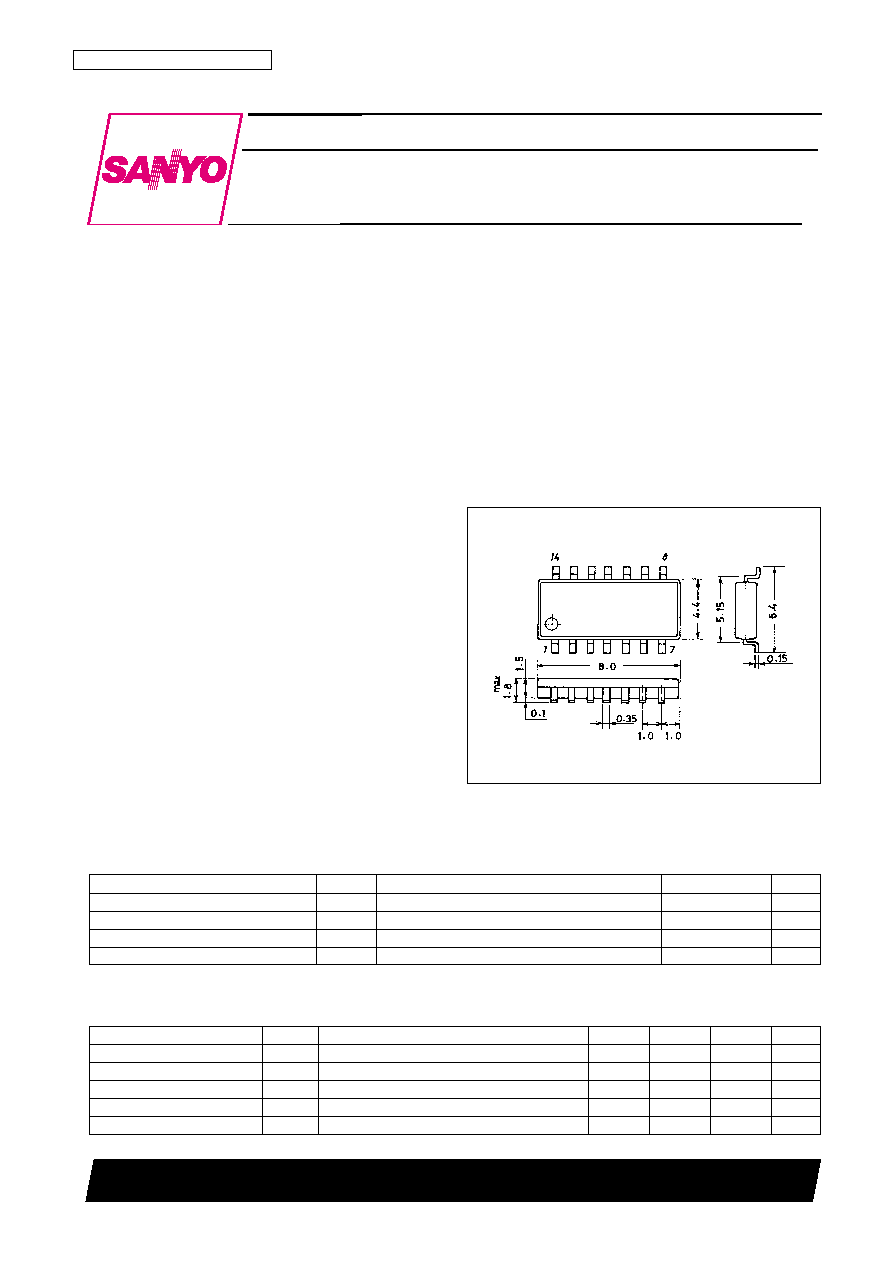
Package Dimensions
unit: mm
3111-MFP14S
Preliminary
SANYO: MFP14S
[LC89975M]
LC89975M
SANYO Electric Co.,Ltd. Semiconductor Bussiness Headquarters
TOKYO OFFICE Tokyo Bldg., 1-10, 1 Chome, Ueno, Taito-ku, TOKYO, 110-0005 JAPAN
PAL-Format Delay Line
NMOS + CCD
Specifications
Absolute Maximum Ratings
at Ta = 25∞C
Recommended Conditions
at Ta = 25∞C
Parameter
Symbol
Conditions
Ratings
Unit
Supply voltage
V
DD
≠0.3 to +6.0
V
Allowable power dissipation
Pdmax
250
mW
Operating temperature
Topr
≠10 to +60
∞C
Storage temperature
Tstg
≠55 to +150
∞C
Parameter
Symbol
Conditions
min
typ
max
Unit
Supply voltage
V
DD
4.75
5.00
5.25
V
Clock input amplitude
V
CLK
300
500
1000
mVp-p
Clock frequency
F
CLK
Sine wave
--
4.43361875
--
MHz
Chrominance signal input amplitude
V
IN-C
--
350
500
mVp-p
Luminance signal input amplitude
V
IN-Y
--
400
572
mVp-p
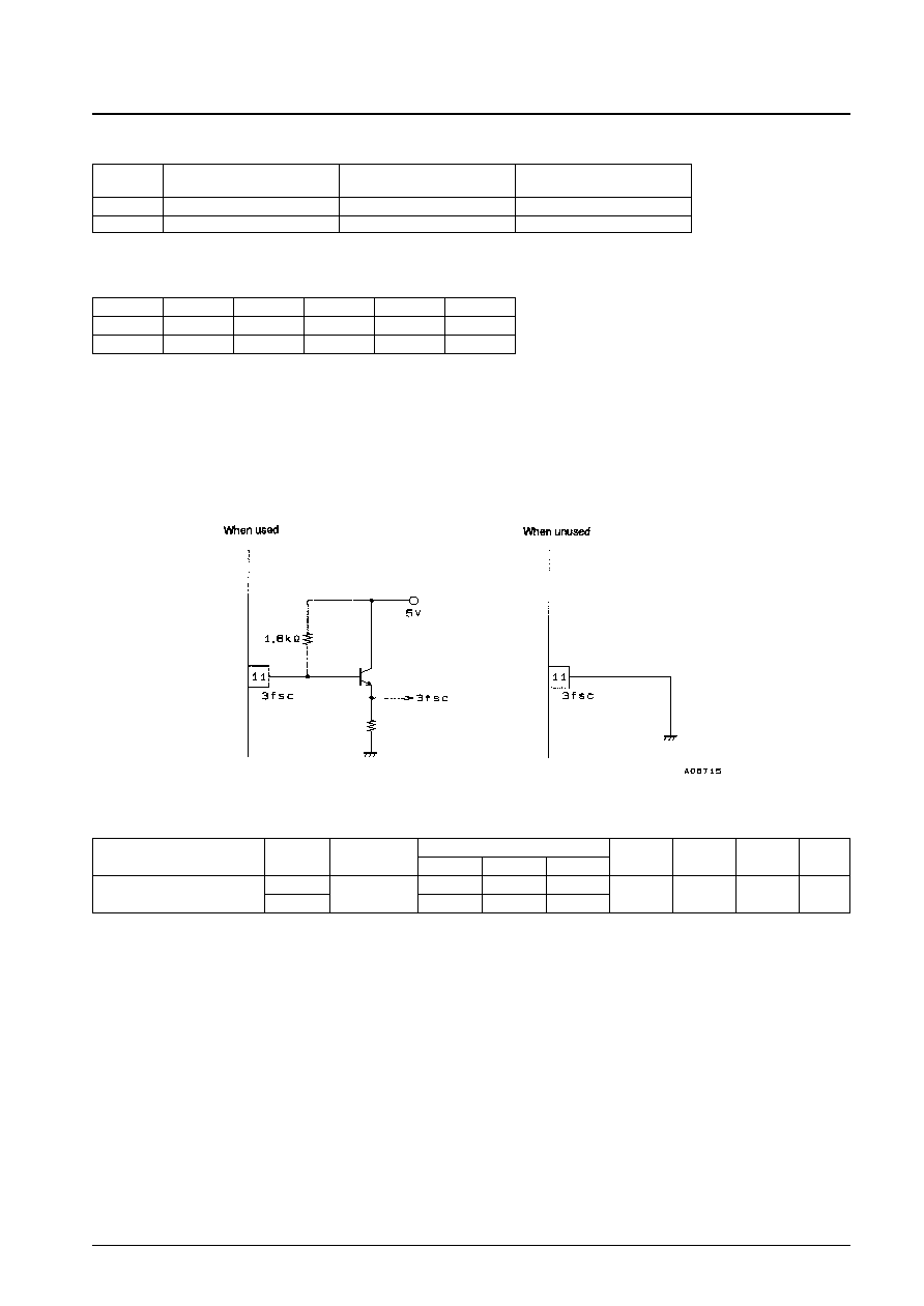
Control Pin
Switching levels
Note: Since a pull-down resistor of about 70 k
is built in the control pin circuit, it will remain fixed at the low level if
left open.
3fsc Pin
This pin outputs the 3∑fsc clock signal generated by the PLL 3
◊
circuit.
Electrical Characteristics
at V
DD
= 5.0 V, Ta = 25∞C, F
CLK
= 4.43361875 MHz, V
CLK
= 500 mVp-p
No. 5391-3/7
LC89975M
CONT
Mode
Chrominance signal delay
Luminance signal delay
(typical example)
(number of CCD stages)
(number of CCD stages)
Low
PAL/GBI
2H (1705) + 0H (2.5)
1H (849)
High
4.43 NTSC
1H (847) + 0H (2.5)
1H (843)
Low/High
Symbol
min
typ
max
Unit
Low
V
L
≠0.3
0.0
+0.5
V
High
V
H
2.0
5.0
6.0
V
Parameter
Symbol
Test conditions
Switch states
min
typ
max
Unit
SW1
SW2
SW3
Power-supply current
I
DD-1
1
a
a
b
27
32
37
mA
I
DD-2
b
a
b
Test Conditions
1. Power-supply current with no input signal applied
2. Pin output voltage with no input signal applied (center bias voltage)
3. Measure the C-OUT output when 350-mVp-p sine wave signals are input to C-IN1 and C-IN2.
G
VC
= 20 log
[dB]
Measured frequencies
G
VC-1
4.429662 MHz
(PAL/GBI)
G
VC-2
4.425694 MHz
(4.43 NTSC)
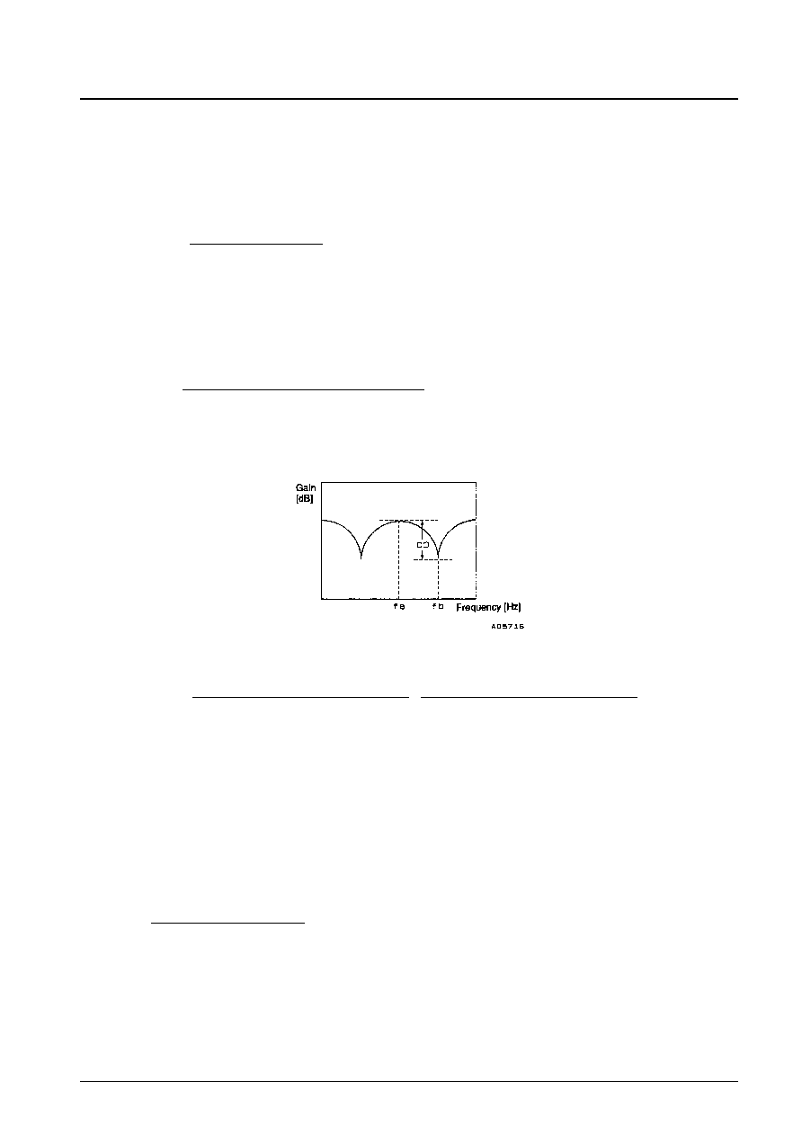
4. Measure the comb depth from the C-OUT output when 350-mVp-p sine wave signals of frequency fa are input to C-
IN1 and C-IN2 and when signals of frequency fb are input.
C
D
= 20 log
[dB]
Measured frequencies
fa
fb
C
D-1
4.429662 MHz
4.425756 MHz
(PAL/GBI)
C
D-2
4.425694 MHz
4.417819 MHz
(4.43 NTSC)
5. Measure the C-OUT output when 200-mVp-p sine wave signals are input to C-IN1 and C-IN2 and when 500-mVp-p
sine wave signals are input and calculate the gain difference.
L
NC
= 20 log
(
/
)
[dB]
Measured frequencies
L
NC-1
4.429662 MHz
(PAL/GBI)
L
NC-2
4.425694 MHz
(4.43 NTSC)
6. Measure the 3∑fsc (13.3 MHz) and fsc (4.43 MHz) components in the C-OUT output with no input signal applied.
7. Measure the noise in the C-OUT output with no input signal applied.
Set up the noise meter with a 200-kHz high-pass filter and a 5-MHz low-pass filter.
8. Let V1 be the C-OUT output when 350-mVp-p sine wave signals are input to C-IN1 and C-IN2 with SW3 in the a
position, and V2 be the C-OUT output with SW3 in the b position.
Z
OC
=
◊
500 [
]
Measured frequencies
Z
OC-1
4.429662 MHz
(PAL/GBI)
Z
OC-2
4.425694 MHz
(4.43 NTSC)
V2 [mVp-p] ≠ V1 [mVp-p]
V1 [mVp-p]
Output for a 200-mVp-p input [mVp-p]
200 [mVp-p]
Output for a 500-mVp-p input [mVp-p]
500 [mVp-p]
The C-OUT output for an fb input [mVp-p]
The C-OUT output for an fa input [mVp-p]
C-OUT output [mVp-p]
350 [mVp-p]
No. 5391-5/7
LC89975M