 | –≠–ª–µ–∫—Ç—Ä–æ–Ω–Ω—ã–π –∫–æ–º–ø–æ–Ω–µ–Ω—Ç: LC89978M | –°–∫–∞—á–∞—Ç—å:  PDF PDF  ZIP ZIP |
Overview
The LC89978M is a CCD delay line for multi television
system that incorporates a comb filter to remove noise
from the chrominance signal and a 1-H delay line for the
luminance signal.
Features
∑ 5-V single-voltage power supply
∑ Built-in 4
◊
PLL frequency multiplier circuit allows 4fsc
operation from an fsc (3.58 MHz) input.
∑ Can be switched between the NTSC/M, PAL/GBI, and
PAL/M formats by setting control pin values.
∑ Includes a built-in crosstalk exclusion comb filter for the
chrominance signal that provides high-precision comb
characteristics in an adjustment-free circuit.
∑ Peripheral circuits provided on chip for operation with a
minimum of external components.
∑ Positive-phase signal input, positive-phase signal output
(luminance signal)
Functions
∑ CCD shift registers (for chrominance and luminance
signals)
∑ Timing generator and clock driver for CCD
∑ Delay time selective circuit
∑ CCD signal adder
∑ Auto-bias circuit
∑ Sync tip clamp circuit (luminance signal)
∑ Center bias circuit (chrominance signal)
∑ Sample-and-hold circuit
∑ 4
◊
PLL frequency multiplier circuit
∑ 4fsc clock output circuit
∑ High voltage generator for CCD Reset Drain (RD).
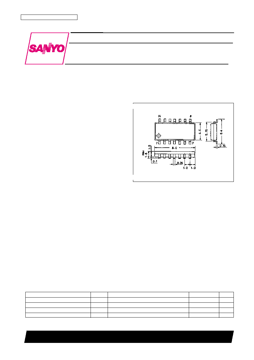
Package Dimensions
unit: mm
3111-MFP14S
CMOS LSI
Ordering number : EN5546A
73097HA (OT)/N3096HA (OT) No. 5546-1/7
SANYO: MFP14S
[LC89978M]
SANYO Electric Co.,Ltd. Semiconductor Bussiness Headquarters
TOKYO OFFICE Tokyo Bldg., 1-10, 1 Chome, Ueno, Taito-ku, TOKYO, 110 JAPAN
CCD Delay Line for Multi-System
LC89978M
Parameter
Symbol
Conditions
Ratings
Unit
Supply voltage
V
DD
≠0.3 to +6.0
V
Allowable power dissipation
Pd max
250
mW
Operating temperature
Topr
≠10 to +60
∞C
Storage temperature
Tstg
≠55 to +125
∞C
Specifications
Absolute Maximum Ratings
at Ta = 25∞C

No. 5546-2/7
LC89978M
Parameter
Symbol
Conditions
Ratings
Unit
min
typ
max
Supply voltage
V
DD
4.75
5.00
5.25
V
Clock input amplitude
V
CLK
300
500
1000
mVp-p
Clock frequency
F
CLK
Sine wave
3.579545
MHz
Chrominance signal input amplitude
V
IN-C
350
500
mVp-p
Luminance signal input amplitude
V
IN-Y
400
572
mVp-p
Allowable Operating Ranges
at Ta = 25∞C
Pin Assignment
Block Diagram
No. 5546-3/7
LC89978M
CONT1
CONT2
Mode (representative)
Chrominance signal delay (number of CCD stages)
Luminance signal delay (number of CCD stages)
Low
Low
PAL/GBI
2H (1833.5) + 0H (1.5)
1H (913)
Low
High
PAL/M
2H (1821.5) + 0H (1.5)
1H (907)
High
Low
--
--
--
High
High
NTSC/M
1H (911.5) + 0H (1.5)
1H (907)
Control Pin Functions
Parameter
Symbol
Conditions
Ratings
Unit
min
typ
max
Switching voltage level: low
V
L
≠0.3
0.0
+0.5
V
Switching voltage level: high
V
H
2.0
5.0
6.0
V
Switching Voltage Levels
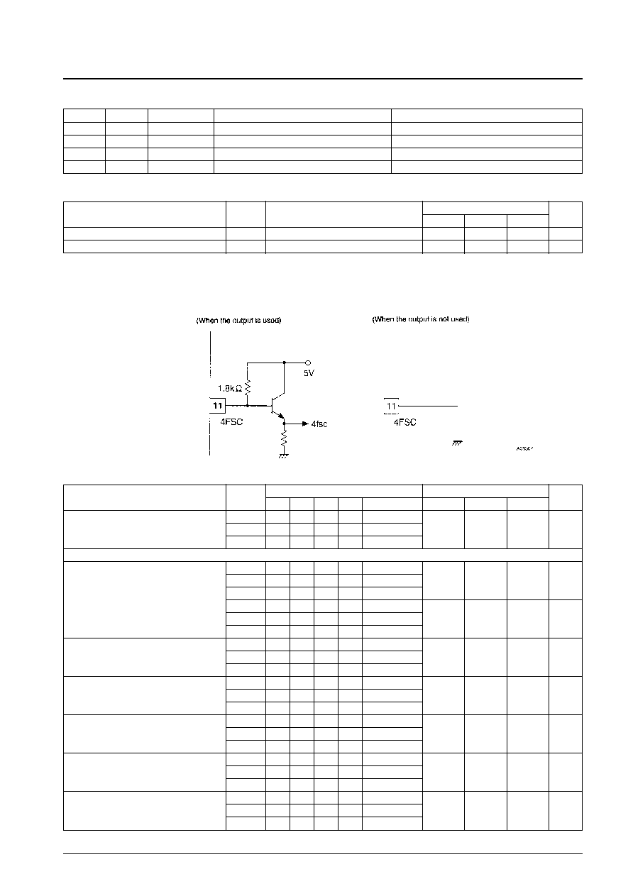
Function of the 4FSC Pin
This pin provides a 4fsc clock signal generated by the 4
◊
PLL frequency multiplier circuit.
Note:
*
Since the control pins have built-in pull-down resistors (about 70 k
), leaving these pins opens effectively sets them to the low level.
Continued on next page.
Parameter
Symbol
Switch states
Ratings
Unit
SW1
SW2
SW3
SW4
Test conditions
min
typ
max
I
DD-1
a
a
a
b
*
1
Supply current
I
DD-2
a
b
a
b
*
1
31
36
41
mA
I
DD-3
b
b
a
b
*
1
[Chrominance signal characteristics] (with no input to Y-IN)
V
INC-1
a
a
a
b
*
2
V
INC-2
a
b
a
b
*
2
1.9
2.4
2.9
V
DC output voltage
V
INC-3
b
b
a
b
*
2
V
OUTC-1
a
a
a
b
*
2
V
OUTC-2
a
b
a
b
*
2
1.4
1.9
2.4
V
V
OUTC-3
b
b
a
b
*
2
G
VC-1
a
a
a
b
*
3
Voltage gain
G
VC-2
a
b
a
b
*
3
≠2
0
+2
dB
G
VC-3
b
b
a
b
*
3
C
D-1
a
a
a
b
*
4
Comb depth
C
D-2
a
b
a
b
*
4
≠40
≠35
dB
C
D-3
b
b
a
b
*
4
L
NC-1
a
a
a
b
*
5
Linearity
L
NC-2
a
b
a
b
*
5
≠0.3
0.0
+0.3
dB
L
NC-3
b
b
a
b
*
5
L
CK4C-1
a
a
a
b
*
6
Clock leakage (4fsc)
L
CK4C-2
a
b
a
b
*
6
10
50
mVrms
L
CK4C-3
b
b
a
b
*
6
L
CK1C-1
a
a
a
b
*
6
Clock leakage (fsc)
L
CK1C-2
a
b
a
b
*
6
0.5
1.5
mVrms
L
CK1C-3
b
b
a
b
*
6
Electrical Characteristics
at V
DD
= 5.0 V, Ta = 25∞C, F
CLK
= 3.579545 MHz, V
CLK
= 500 mVp-p
No. 5546-4/7
LC89978M
Continued from preceding page.
Parameter
Symbol
Switch states
Ratings
Unit
SW1
SW2
SW3
SW4
Test conditions
min
typ
max
N
C-1
a
a
a
b
*
7
Noise
N
C-2
a
b
a
b
*
7
0.5
2.0
mVrms
N
C-3
b
b
a
b
*
7
Z
OC-1
a
a
a
a, b
*
8
Output impedance
Z
OC-2
a
b
a
a, b
*
8
200
350
500
Z
OC-3
b
b
a
a, b
*
8
T
DC-1
a
a
a
b
*
9
0-H delay time
T
DC-2
a
b
a
b
*
9
160
ns
T
DC-3
b
b
a
b
*
9
[Luminance signal characteristics] (With no signals input to C-IN1 and C-IN2)
V
INY-1
a
a
a
b
*
10
V
INY-2
a
b
a
b
*
10
1.3
1.8
2.3
V
DC output voltage
V
INY-3
b
b
a
b
*
10
V
OUTY-1
a
a
a
b
*
10
V
OUTY-2
a
b
a
b
*
10
0.7
1.2
1.7
V
V
OUTY-3
b
b
a
b
*
10
G
VY-1
a
a
a
b
*
11
Voltage gain
G
VY-2
a
b
a
b
*
11
≠2
0
+2
dB
G
VY-3
b
b
a
b
*
11
G
FY-1
a
a
b
b
*
12
Frequency response
G
FY-2
a
b
b
b
*
12
≠2
0
+2
dB
G
FY-3
b
b
b
b
*
12
D
GY-1
a
a
a
b
*
13
Differential gain
D
GY-2
a
b
a
b
*
13
0
5
8
%
D
GY-3
b
b
a
b
*
13
D
PY-1
a
a
a
b
*
13
Differential phase
D
PY-2
a
b
a
b
*
13
0
5
8
deg
D
PY-3
b
b
a
b
*
13
L
SY-1
a
a
a
b
*
14
Linearity
L
SY-2
a
b
a
b
*
14
37
40
43
%
L
SY-3
b
b
a
b
*
14
L
CK4Y-1
a
a
a
b
*
15
Clock leakage (4fsc)
L
CK4Y-2
a
b
a
b
*
15
10
50
mVrms
L
CK4Y-3
b
b
a
b
*
15
L
CK1Y-1
a
a
a
b
*
15
Clock leakage (fsc)
L
CK1Y-2
a
b
a
b
*
15
0.5
1.5
mVrms
L
CK1Y-3
b
b
a
b
*
15
N
Y-1
a
a
a
b
*
16
Noise
N
Y-2
a
b
a
b
*
16
0.5
2.0
mVrms
N
Y-3
b
b
a
b
*
16
Z
OY-1
a
a
a
c, b
*
17
Output impedance
Z
OY-2
a
b
a
c, b
*
17
250
400
550
Z
OY-3
b
b
a
c, b
*
17
T
DY-1
a
a
a
b
*
18
63.81
µs
Delay time
T
DY-2
a
b
a
b
*
18
63.39
µs
T
DY-3
b
b
a
b
*
18
63.39
µs
Test Conditions
1. The supply current with no input signal
2. The pin output voltage (the center bias voltage) with no input signal
3. Measure the C-OUT output when a 350-mVp-p sine wave is input to C-IN1 and C-IN2.
C-OUT output [mVp-p]
G
VC
= 20log -------------------- [dB]
350 [mVp-p]
Test frequencies:
G
VC-1
: 4.431395 MHz (PAL/GBI)
G
VC-2
: 3.571628 MHz (PAL/M)
G
VC-3
: 3.571628 MHz (NTSC/M)
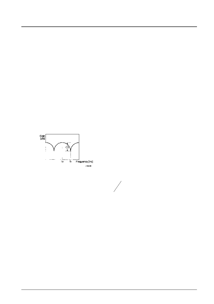
4. Measure the comb depth from the C-OUT output when a 350-mVp-p sine wave with frequency fa is input to C-IN1
and C-IN2, and when a sine wave of frequency fb is input.
The C-OUT output for an fb input [mVp-p]
C
D
= 20log ------------------------------------ [dB]
The C-OUT output for an fa input [mVp-p]
Test Frequencies
fa
fb
C
D-1
: 4.431395 MHz (PAL/GBI)
4.435303 (PAL/GBI)
G
D-2
: 3.571628 MHz (PAL/M)
3.575561 (PAL/M)
G
D-3
: 3.571628 MHz (NTSC/M)
3.563761 (NTSC/M)
5. Measure the C-OUT output when a 200-mVp-p sine wave is input to C-IN1 and C-IN2, and when a 500-mVp-p sine
wave is input, and calculate the gain difference as follows:
The output for a 500-mVp-p input [mVp-p]
The output for a 200-mVp-p input [mVp-p]
L
NC
= 20log
------------------------------------
------------------------------------ [dB]
500 [mVp-p]
200 [mVp-p]
Test Frequencies
L
NC-1
4.431395MHz (PAL/GBI)
L
NC-2
3.571628MHz (PAL/M)
L
NC-3
3.571628MHz (NTSC/M)
6. Measure the 4fsc (14.3 MHz) and fsc (3.58 MHz) components in the C-OUT output with no input signal.
7. Measure the noise in the C-OUT output with no input signal.
Measure the noise with a noise meter with a 200-kHz high-pass filter and a 5-MHz low-pass filter.
8. Input a 350-mVp-p sine wave to C-IN1 and C-IN2. Let V1 be the C-OUT output when SW3 is set to the `a' position,
and let V2 be the C-OUT output when SW3 is set to the 'b' position.
V2 [mVp-p] ≠ V1 [mVp-p]
Z
OC
= ----------------------
◊
500 [dB]
V1 [mVp-p]
Test Frequencies
Z
OC-1
: 4.431395 MHz (PAL/GBI)
Z
OC-2
: 3.571628 MHz (PAL/M)
Z
OC-3
: 3.571628 MHz (NTSC/M)
9. The delay time in the C-OUT output with respect to the C-IN1 input. This is the CCD 1.5-bit delay.
10. The pin output voltage (clamp voltage) with no input signal.
No. 5546-5/7
LC89978M
(
)