Ordering number : EN
*
5281A
22896HA (OT) No. 5281-1/6
Overview
The LC99012A-S is a timing generator for the 1/5-inch
LC9947G and LC9948G and the 1/6-inch LC9949G
black-and-white CCD image sensors.
Features
∑ 5 V single-voltage power supply
∑ Generates all pulses required for CCD drivers.
∑ Generates all pulses required for video signal
processing.
∑ Built-in synchronizing signal generator that supports
both EIA and CCIR.
∑ Includes buffer circuits for directly driving the CCD
horizontal transfer and reset gates.
∑ Includes light metering and control systems for an
automatic electronic iris function.
∑ Fixed rate-of-change control allows a smooth electronic
iris function to be implemented (an iris state output is
provided).
∑ Supports AGC control and a light metering mode that
compensates for backlighting.
∑ Selectable CCD storage mode (non-interlaced or
interlaced)
∑ Selectable TV scan mode (non-interlaced or interlaced)
∑ Allows all types of external synchronization.
∑ Built-in EXT-C.SYNC sync separator circuit
∑ Built-in phase comparator for external synchronization
∑ Control from external electronic shutter pulses and
frame shift pulses supports one-shot imaging.
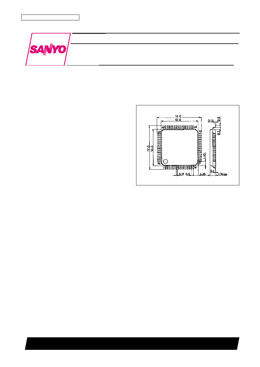
∑ Package: 0.5 mm lead pitch flat package (SQFP-64)
∑ Flickerless function
∑ Sensitivity-increasing function
Package Dimensions
unit: mm
3190-SQFP64
Preliminary
SANYO: SQFP64
[LC99012A-S]
LC99012A-S
SANYO Electric Co.,Ltd. Semiconductor Bussiness Headquarters
TOKYO OFFICE Tokyo Bldg., 1-10, 1 Chome, Ueno, Taito-ku, TOKYO, 110-8534 JAPAN
Black-and-White CCD Timing Generator
CMOS LSI
Specifications
Absolute Maximum Ratings
at V
SS
= 0 V
Note:
*
Per individual I/O reference cell
Allowable Operating Ranges
at Ta = ≠30 to +65įC, V
SS
= 0 V
DC Characteristics: Input and Output Levels
at V
SS
= 0 V, V
DD
= 4.5 to 5.5 V, Ta = ≠30 to +65įC
See the note on next page.
No. 5281-2/6
LC99012A-S
Parameter
Symbol
Conditions
Ratings
Unit
Maximum supply voltage
V
DD
max
≠0.3 to +7.0
V
Input and output voltages
V
I
, V
O
≠0.3 to V
DD
+ 0.3
V
Allowable power dissipation
Pd max
Ta
65įC
290
mW
Operating temperature
Topr
≠30 to +65
įC
Storage temperature
Tstg
≠55 to +125
įC
Soldering heat resistance
Hand soldering: 3 seconds
350
įC
Reflow soldering: 10 seconds
235
įC
Input and output currents
I
I
, I
O
Ī20
*
mA
Parameter
Symbol
Conditions
min
typ
max
Unit
Supply voltage
V
DD
4.5
5.0
5.5
V
Input voltage range
V
IN
0
V
DD
V
Parameter
Symbol
Conditions
min
typ
max
Unit
Input high-level voltage
V
IH
1
TTL levels: (6)
2.2
V
Input low-level voltage
V
IL
1
TTL levels: (6)
0.8
V
Input high-level voltage
V
IH
2
CMOS levels: (1), (3)
0.7 V
DD
V
Input low-level voltage
V
IL
2
CMOS levels: (1), (3)
0.3 V
DD
V
Input high-level voltage
V
IH
3
CMOS levels, Schmitt inputs: (4)
0.8 V
DD
V
Input low-level voltage
V
IL
3
CMOS levels, Schmitt inputs: (4)
0.2 V
DD
V
Input high-level voltage
V
IH
4
CMOS levels, inputs with pull-up resistors: (2)
0.7 V
DD
V
Input low-level voltage
V
IL
4
CMOS levels, inputs with pull-up resistors: (2)
0.3 V
DD
V
Input high-level voltage
V
IH
5
CMOS levels, inputs with pull-up resistors: (5)
0.7 V
DD
V
Input low-level voltage
V
IL
5
CMOS levels, inputs with pull-up resistors: (5)
0.3 V
DD
V
Output high-level voltage
V
OH
1
I
OH
= ≠3 mA: (6), (13), (14), (15)
V
SS
≠ 2.1
V
Output low-level voltage
V
OL
1
I
OL
= 3 mA: (6), (13), (14), (15)
0.4
V
Output low-level voltage
V
OL
2
I
OL
= 3 mA: (9)
0.4
V
Output high-level voltage
V
OH
3
I
OH
= ≠6 mA: (12)
V
DD
≠ 2.1
V
Output low-level voltage
V
OL
3
I
OL
= 6 mA: (12)
0.4
V
Output high-level voltage
V
OH
4
I
OH
= ≠6 mA: (7)
V
DD
≠ 2.1
V
Output low-level voltage
V
OL
4
I
OL
= 2 mA: (7)
0.4
V
Output high-level voltage
V
OH
5
I
OH
= ≠30 mA: (11)
V
DD
≠ 2.1
V
Output low-level voltage
V
OL
5
I
OL
= 10 mA: (11)
0.4
V
Output high-level voltage
V
OH
6
I
OH
= ≠12 mA: (8)
V
DD
≠ 2.1
V
Output low-level voltage
V
OL
6
I
OL
= 12 mA: (8)
0.4
V
Output high-level voltage
V
OH
6
I
OH
= ≠12 mA: (10)
V
DD
≠ 1.5
V
Output low-level voltage
V
OL
7
I
OL
= 6 mA: (8)
0.4
V
Input leakage current
I
IL
V
I
= V
SS
, V
DD
: (1), (3), (4), (6)
≠10
+10
ĶA
Output leakage current
I
OZ
In high-impedance output mode: (6), (9), (13)
≠10
+10
ĶA
Pull-up resistance
R
UP
(2)
10
20
40
k
Pull-down resistance
R
DN
(5)
25
50
100
k
Note: The applicable pin sets are defined as follows:
Input
(1) ......AI, CKI
(2) ......FLESS, STR, TEST
(3) ......EXT1, EXT2, KISYU, TV
(4) ......HR, SELMET1, SELMET2, VR
(5) ......CCDSCAN, EXT3, EXT4, MSENS, SENS, SSGSCAN
I/O
(6) ......STEPSTOP
Output
(7) ......PCO
(8) ......DHTR
(9) ......IRRES
(10) ....A0, CKO
(11) ....DHT1, DHT2
(12) ....DS1, DS2
(13) ....AGCC2, IRSTA
(14) ....CLK14M, CLP1, CLP2, FLD, HD, NSUB1, NSUB2, VD
(15) ....CBLK, C.SYNC, NSUB3, PBLK, VI1 to VI4, VS1 to VS4
*
......VIDI, VIDO, DCH, DCL, IRIS (These pins are not covered in the DC characteristics.)
Pin Assignment
I/O
I: Input pin, O: Output pin, B: Bidirectional pin, P: Power supply pin, NC: Unconnected pin
Note: All V
DD
and V
SS
pins must be connected to the power supply or ground. Do not leave any of these pins open.
No. 5281-3/6
LC99012A-S
No.
Symbol
I/O
No.
Symbol
I/O
1
V
SS
P
64
DCL
I
2
PCO
O
63
DCH
I
3
AI
I
62
IRIS
I
4
AO
O
61
IRRES
O
5
CKI
I
60
VIDO
O
6
CKO
O
59
VIDI
I
7
CCDSCAN
I
58
IRSTA
O
8
SSGSCAN
I
57
AGCC2
O
9
CLK14M
O
56
V
DD
P
10
HD
O
55
TV
I
11
VD
O
54
C.SYNC
O
12
FLD
O
53
CBLK
O
13
V
DD
P
52
PBLK
O
14
KISYU
I
51
CLP2
O
15
HR
I
50
CLP1
O
16
VR
I
49
V
SS
P
17
V
SS
P
48
DS1
O
18
SELMET1
I
47
DS2
O
19
SELMET2
I
46
V
DD
P
20
EXT1
I
45
DHT2
O
21
EXT2
I
44
DHT1
O
22
EXT3
I
43
DHTR
O
23
EXT4
I
42
V
SS
P
24
V
DD
P
41
VS3
O
25
STEPSTOP
B
40
VS2
O
26
SENS
I
39
VS1
O
27
MSENS
I
38
VS4
O
28
FLESS
I
37
VI4
O
29
STR
I
36
VI2
O
30
NSUB3
O
35
VI3
O
31
NSUB2
O
34
VI1
O
32
NSUB1
O
33
TEST
I
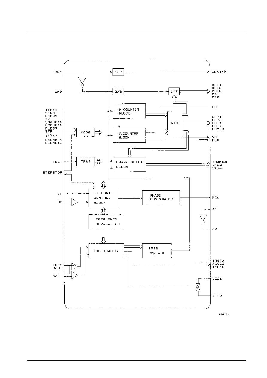
Block Diagram
No. 5281-4/6
LC99012A-S
Pin Functions
Note:
*
Flickerless mode can be used when the auto-iris function is off, i.e. when EXT3 is high and EXT4 is low.
No. 5281-5/6
LC99012A-S
Pin No.
Symbol
I/O
Function
1
GND
2
PCO
O
Phase comparator output
3
AI
I
PCO output signal low-pass filter amplifier input
4
AO
O
PCO output signal low-pass filter amplifier output
Reference clock input (resonator inverter input)
5
CKI
I
LC9947G
:
28.63636 MHz
LC9948G: 28.375 MHz
LC9949G: 14.31818 MHz
6
CKO
O
Resonator inverter output
7
CCDSCAN
I
Low/open: CCD interlaced storage mode
High: CCD non-interlaced storage mode
8
SSGSCAN
I
Low/open: C.SYNC interlaced mode
High: C.SYNC non-interlaced mode
9
CLK14M
O
LC9947G/9949G: 14.31818 MHz
LC9948G: 14.1875 MHz
10
HD
O
HD output
11
VD
O
VD output
Field identifier signal
12
FLD
O
High: odd
Low: even
Must be tied high if SSGSCAN is high.
13
V
DD
14
KISYU
I
Must be tied high when used with the LC9949G. Otherwise must be tied low.
15
HR
I
Horizontal reset, C.SYNC reset, and vertical reset pulse input
16
VR
I
Vertical reset pulse input and external synchronization mode setup
17
GND
18
SELMET1
I
Light metering mode control
19
SELMET2
I
Light metering mode control
20
EXT1
I
External synchronization mode control
21
EXT2
I
External synchronization mode control
22
EXT3
I
CCD drive external control mode control
23
EXT4
I
CCD drive external control mode control
24
V
DD
I
Normally used to control the electronic iris step (rate of change)
25
STEPSTOP
I/O
Low: 1/8
Hifh: 1/16
Sensitivity increasing switch
26
SENS
I
Low/open: normal
High: Increased sensitivity mode
Increased sensitivity mode type switching
27
MSENS
I
Low or open: In field units
High: In single scan line (1H) units
Flickerless mode
*
switch
28
FLESS
I
Low: Flickerless mode
High/open: normal
CCD storage mode control
29
STR
I
This pin must be left open or tied high when the LC99012A-S is used with an LC9947G/49G, and must
be tied low when used with an LC9948G.
30
NSUB3
O
CCD NSUB pulses
31
NSUB2
O
CCD NSUB pulses
32
NSUB1
O
CCD NSUB pulses
33
TEST
I
Low: test mode
High/open: normal operating mode
34
VI1
O
CCD imaging block transfer clock (Ý1)
35
VI3
O
CCD imaging block transfer clock (Ý3)
36
VI2
O
CCD imaging block transfer clock (Ý2)
37
VI4
O
CCD imaging block transfer clock (Ý4)
38
VS4
O
CCD imaging block transfer clock (ÝS4)
Continued on next page.