Overview
The LC99063-LF2 is a color video signal processor for
use with the LC9997M/FL.
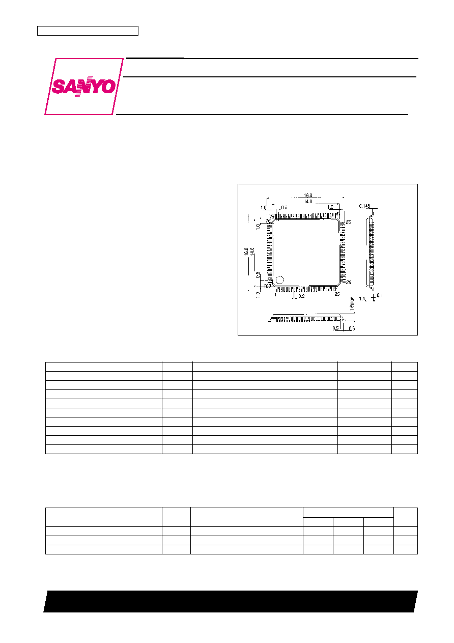
Package Dimensions
unit: mm
3181B-SQFP100
CMOS IC
51398RM (OT) No. 5787-1/8
SANYO: SQFP100
[LC99063-LF2]
SANYO Electric Co.,Ltd. Semiconductor Bussiness Headquarters
TOKYO OFFICE Tokyo Bldg., 1-10, 1 Chome, Ueno, Taito-ku, TOKYO, 110-8534 JAPAN
CCD Digital Signal Processing IC
LC99063-LF2
Ordering number : EN5787
Parameter
Symbol
Conditions
Ratings
Unit
Supply voltage
V
DD
max
≠0.3 to +4.6
V
I/O voltage
V
I
1, V
O
For pin type 1
≠0.3 to V
DD
+0.3
V
Input voltage
V
I
2
For pin type 2
≠0.3 to +7.3
V
Allowable power dissipation
Pd max
400
mW
Operating temperature
Topr
≠15 to +70
∞C
Storage temperature
Tstg
≠55 to +125
∞C
Solder resistance (Hand soldering)
3s
350
∞C
Solder resistance (Reflow)
10s
235
∞C
I/O current
Ii, Io
*
±20
mA
Specifications
Absolute Maximum Ratings
at V
SS
= 0 V
The pin types above refer to the following groups.
(1) DIN[32:9], DEVICE, MIRRO, SUPER, INMODE, WBHL, DOSL, SSET [2:1], OMODE [4:1], RES, DOUT [24:1], HREF, VDO, HDO, CLKOUT, ANA1,
ANA2, IREFOT1, IREFOT2, VREF1, VREF2, COMP1, COMP2
(2) DIN[8:1], CLK14M, CLK10M, HDI, VDI, HREF53, ENS, DATAS, CLKS, REGRES
*
: This value is for a single I/O basic cell.
(1) DIN[32:9], DEVICE, MIRRO, SUPER, INMODE, WBHL, DOSL, SSET [2:1], OMODE [4:1], RES
(2) DIN[8:1], CLK14M, CLK10M, HDI, VDI, HREF53, ENS, DATAS, CLKS, REGRES
Parameter
Symbol
Conditions
Ratings
Unit
min
typ
max
Supply voltage
V
DD
3
3.3
3.6
V
Input voltage range 1
Vin1
For pin type 1
0
V
DD
V
Input voltage range 2
Vin2
For pin type 2
0
+5.3
V
Allowable Operating Ranges
at Ta = ≠15 to +70∞C, V
SS
= 0 V

LC99063-LF2
Parameter
Symbol
Conditions
Ratings
Unit
min
typ
max
Input high-level voltage
V
IH
CMOS level ; for pin type 1
0.7 V
DD
V
Input low-level voltage
V
IL
CMOS level ; for pin type 1
0.2 V
DD
V
Input high-level voltage
V
IH
CMOS level with Schmitt ; for pin type 2
0.75 V
DD
V
Input low-level voltage
V
IL
CMOS level with Schmitt ; for pin type 2
0.15 V
DD
V
Output high-level voltage
V
OH
I
OH
= ≠2 mA; for pin types 3 and 4
V
DD
≠ 0.8
V
Output low-level voltage
V
OL
I
OL
= +2 mA; for pin types 3 and 4
0.4
V
Input leak current
I
L
V
I
= V
DD
; for pin types 1 and 2
≠10
+10
µA
Output leak current
Ioz
High-impedance output; for pin type 3
≠10
+10
µA
Electrical Characteristics for Logic Circuits
DC Characteristics
at Ta = ≠15 to +70∞C, V
DD
= 3.0 to 3.6 V, V
SS
= 0 V
The pin types above refer to the following groups.
INPUT
(1) DIN [32:9], DEVICE, MIRRO, SUPER, INMODE, WBHL, DOSL, SSET [2:1], OMODE [4:1], RES
(2) DIN [8:1], CLK14M, CLK10M, HDI, VDI, HREF53, ENS, DATAS, CLKS, REGRES
OUTPUT
(3) DOUT [24:1]
(4) HREF, VDO, HDO, CLKOUT
Note: The ANA1, ANA2, IREFOT1, IREFOT2, VREF1, VREF2, COMP1, and COMP2 pins fall outside these DC characteristic specifications.
Electrical Characteristics for Analog Circuits
Recommended operating conditions for D/A converter
Parameter
Symbol
Conditions
Ratings
Unit
min
typ
max
Reference voltage
VREF1/2
1.11
V
Analog output resistance
Ra
200
Reference voltage resistance
Ri
Ra
◊
4
Phase compensation capacitor
Cc
0.1
µF
VREF capacitor
Cv
0.1
µF
No. 5787-2/8
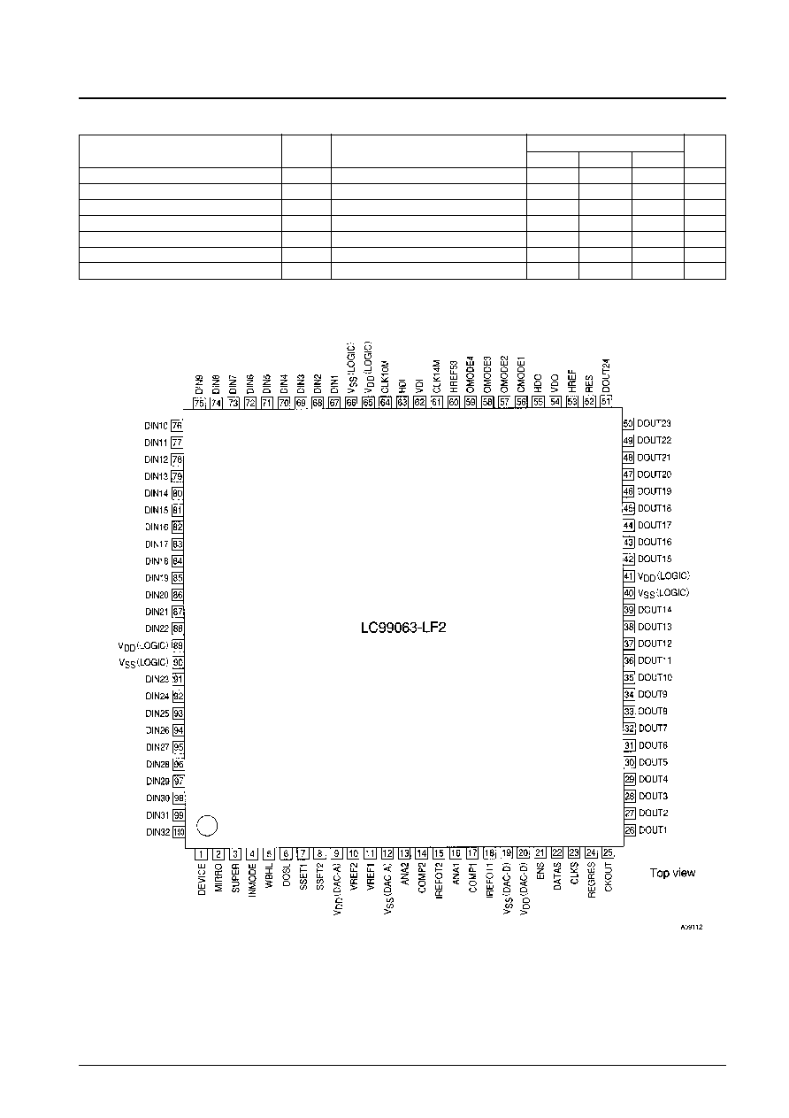
Pin Assignment
No. 5787-3/8
LC99063-LF2
Parameter
Symbol
Conditions
Ratings
Unit
min
typ
max
Resolution
8
Bits
Conversion frequency
15
MSPS
Zero scale output voltage
≠15
0
+15
mV
Full scale output voltage
1.01
1.1
1.19
V
Linearity error
±1.0
LSB
Differential linearity error
±0.5
LSB
Reference output voltage
1.09
1.1
1.11
V
Electrical Characteristics for D/A Converter
at Ta = 25∞C, V
DD
= 3.3 V, Rv = 200
, Ri = 800
No. 5787-4/8
LC99063-LF2
Pin Functions
Pin No.
Symbol
I/O
Function
1
DEVICE
I
0 : LC9997FL 1 : LC9997M
2
MIRRO
I
0 : NORMAL 1 : MIRROR
3
SUPER
I
Superimpose control 0 : Superimpose 1 : Camera through
4
INMODE
I
Input mode select
5
WBHL
I
Auto white balance hold 0 : Hold 1 : Auto
6
DOSL
I
Pin 55 output select 0 : HD 1 : C.SYNC
7
SSET1
I
Color sampling phase select
8
SSET2
I
Color sampling phase select
9
V
DD
(DAC-A)
P
10
VREF2
O
DAC2 reference voltage output
11
VREF1
O
DAC1 reference voltage output
12
V
SS
(DAC-A)
P
13
ANA2
O
DAC2 output
14
COMP2
I
DAC2 bias pin
15
IREFOT2
O
DAC2 reference current
16
ANA1
O
DAC1 output
17
COMP1
I
DAC1 bias pin
18
IREFOT1
O
DAC1 reference current
19
V
SS
(DAC-D)
P
20
V
DD
(DAC-D)
P
21
ENS
I
Serial resister enable
22
DATAS
B
Serial resister data
23
CLKS
I
Serial resister CLK
24
REGRES
I
Serial resister reset
25
CKOUT
O
CCIR601, square PIX mode CLK
26
DOUT1
O
Output Channel1 = CH1 (LSB)
27
DOUT2
O
Output Channel1
28
DOUT3
O
Output Channel1
29
DOUT4
O
Output Channel1
30
DOUT5
O
Output Channel1
31
DOUT6
O
Output Channel1
32
DOUT7
O
Output Channel1
33
DOUT8
O
Output Channel1 = CH1 (MSB)
34
DOUT9
O
Output Channel2 = CH2 (LSB)
35
DOUT10
O
Output Channel2
36
DOUT11
O
Output Channel2
37
DOUT12
O
Output Channel2
38
DOUT13
O
Output Channel2
39
DOUT14
O
Output Channel2
40
V
SS
(logic)
41
V
DD
(logic)
42
DOUT15
O
Output Channel2
43
DOUT16
O
Output Channel2 = CH2 (MSB)
44
DOUT17
O
Output Channel3 = CH3 (LSB)
45
DOUT18
O
Output Channel3
46
DOUT19
O
Output Channel3
47
DOUT20
O
Output Channel3
48
DOUT21
O
Output Channel3
49
DOUT22
O
Output Channel3
50
DOUT23
O
Output Channel3
51
DOUT24
O
Output Channel3 = CH3 (MSB)
52
RES
I
0 : Test 1 : Real
53
HREF
O
Horizontal reference
54
VDO
O
VD output
55
HDO
O
HD or C.SYNC output
Continued on next page.

No. 5787-5/8
LC99063-LF2
Pin No.
Symbol
I/O
Function
56
OMODE1
I
57
OMODE2
I
Output mode select
58
OMODE3
I
59
OMODE4
I
60
HREF53
I
Horizontal reference (from LC99053)
61
CLK14M
I
FSC4 (LC99053 pin 58), VD (LC99053 pin 56), HD (LC99053 pin 55)
62
VDI
I
or HTCLK (LC99053 pin 51), fixed at high level, C.SYNC (LC99053 pin 54)
63
HDI
I
64
CLK14M
I
HTCLK (LC99053 pin 51)
65
V
DD
(logic)
P
66
V
SS
(logic)
P
67
DIN1
I
8 bit data input (from LC99053) [LSB]
68
DIN2
I
8 bit data input
69
DIN3
I
8 bit data input
70
DIN4
I
8 bit data input
71
DIN5
I
8 bit data input
72
DIN6
I
8 bit data input
73
DIN7
I
8 bit data input
74
DIN8
I
8 bit data input (from LC99053) [MSB]
75
DIN9
I
8 bit Y input [LSB]
76
DIN10
I
8 bit Yinput
77
DIN11
I
8 bit Y input
78
DIN12
I
8 bit Y input
79
DIN13
I
8 bit Y input
80
DIN14
I
8 bit Y input
81
DIN15
I
8 bit Y input
82
DIN16
I
8 bit Y input [MSB]
83
DIN17
I
8 bit U or UV input [LSB]
84
DIN18
I
8 bit U or UV input
85
DIN19
I
8 bit U or UV input
86
DIN20
I
8 bit U or UV input
87
DIN21
I
8 bit U or UV input
88
DIN22
I
8 bit U or UV input
89
V
DD
(logic)
P
90
V
SS
(logic)
P
91
DIN23
I
8 bit U or UV input
92
DIN24
I
8 bit U or UV input [MSB]
93
DIN25
I
8 bit V input [LSB]
94
DIN26
I
8 bit V input
95
DIN27
I
8 bit V input
96
DIN28
I
8 bit V input
97
DIN29
I
8 bit V input
98
DIN30
I
8 bit V input
99
DIN31
I
8 bit V input
100
DIN32
I
8 bit V input [MSB]
Continued from preceding page.