 | –≠–ª–µ–∫—Ç—Ä–æ–Ω–Ω—ã–π –∫–æ–º–ø–æ–Ω–µ–Ω—Ç: LC99104 | –°–∫–∞—á–∞—Ç—å:  PDF PDF  ZIP ZIP |
Ordering number : ENN6247
D1599TH (OT)/30899TH (OT) No. 6247-1/9
Overview
The LC99104 is a black-and-white VGA frame transfer
CCD solid-state imaging device for 1/4-inch optical
systems. It was developed for use in consumer image
input products.
Features
∑ VGA format compatible
∑ Reads each pixel independently
∑ Horizontal dual read method (Each horizontal line is
read twice: odd line and even line; Therefore, signal
processing requires line memory.)
∑ Variable speed electronic shutter possible (1/8 to 1/4000 s)
Device Structure
∑ Effective pixel count [total pixels] :
654H
◊
490V [710H
◊
510V]
∑ Number of optical black pixels :
H direction : 44 pixels in front, 12 pixels in back
V direction : 8 pixels above, 12 pixels below
∑ Dummy bit : H direction 4 pixels
∑ Unit cell size : 5.55 µm (H)
◊
5.55 µm (V)
∑ Square lattice
∑ Parallel gate type CCD sensor
∑ Both imaging block and storage block are composed of
710H
◊
510V pixels
∑ 3-phase drive for imaging block and storage block,
2-phase drive for horizontal block
∑ Built-in high-sensitivity output amplifier
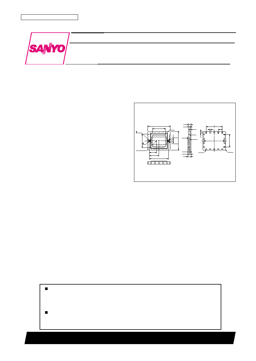
Package Dimensions
unit: mm
3242
LC99104
SANYO Electric Co.,Ltd. Semiconductor Company
TOKYO OFFICE Tokyo Bldg., 1-10, 1 Chome, Ueno, Taito-ku, TOKYO, 110-8534 JAPAN
1/4-Inch Optical Size Frame Transfer Type
VGA Compatible B/W Image Sensor
11.8
10.16
0.7
2.54
1.0
7.62
R0.3
R0.25
1.49
1.05
0.44
0.635
1.075
2.0
Resin
Glass
Sensor
4.53
6.0
12.3
14.3
8.0
8.6
1.2
1.015
Optical Center
1.0
(1.2)
R1.0
(R0.6)
(R0.5)
[LC99104]
Any and all SANYO products described or contained herein do not have specifications that can handle
applications that require extremely high levels of reliability, such as life-support systems, aircraft's
control systems, or other applications whose failure can be reasonably expected to result in serious
physical and/or material damage. Consult with your SANYO representative nearest you before using
any SANYO products described or contained herein in such applications.
SANYO assumes no responsibility for equipment failures that result from using products at values that
exceed, even momentarily, rated values (such as maximum ratings, operating condition ranges, or other
parameters) listed in products specifications of any and all SANYO products described or contained
herein.
No. 6247-2/9
LC99104
Parameter
Symbol
Conditions
Ratings
Unit
Supply voltage
V
DD
, V
RD
V
PW
= 0 V
≠ 0.3 to + 18
V
Load gate voltage
V
GG
V
PW
= 0 V
≠ 0.3 to + 3
V
N-substrate-P-well voltage
NSUB-PW
V
PW
= 0 V
≠ 0.3 to + 50
V
N-substrate-imaging block voltage
NSUB
¯1 to ¯3, ¯S1 to ¯S3, TG1, TG2: V
PW
= 0 V
≠ 0.3 to + 55
V
Horizontal clock, reset gate voltage
V
RD
Horizontal clock pin, ¯R: V
PW
= 0
≠ 0.3 to + 18
V
Clock voltage
Clock pins other than listed above, V
PW
= 0 V
≠ 15 to + 18
V
Pin voltage
Pins other than listed above, V
PW
= 0 V
≠ 0.3 to + 10
V
Operating temperature
Topr
≠10 to +60
∞C
Storage temperature
Tstg
≠30 to +80
∞C
Specifications
Absolute Maximum Ratings
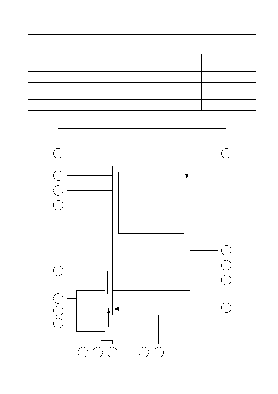
Block Diagram
1
VPW
2
¯3
3
¯2
4
¯1
5
TG1
7
VRD
8
VDD
9
VOUT
10
VGG
12
¯H2
13
¯H1
18
NSUB
17
¯S1
16
¯S2
15 ¯S3
14 TG2
6
¯R
11
VOG
A12552
Optical black block
Imaging block
Storage block
Transfer gate
Horizontal shift register (CCD)
Output block
4 dummy bits
No. 6247-3/9
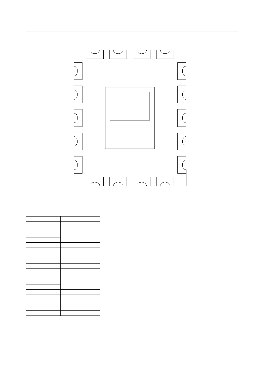
LC99104
Pin Assignment
¯2
3
¯1
4
TG1
5
¯R
6
VRD
7
¯H2
12
¯H1
13
TG2
14
¯S3
15
¯S2
16
VDD
8
VOUT
9
VGG
(Top view)
10
VOG
11
¯3
2
VPW
1
NSUB
18
¯S1
17
A12553
Pin Description
Pin No.
Symbol
Pin Description
1
V
PW
P well
2
¯3
3
¯2
Imaging block clock
4
¯1
5
TG1
Transfer gate
6
¯R
Reset gate
7
V
RD
Reset drain
8
V
DD
Supply voltage
9
V
OUT
CCD output
18
NSUB
N substrate
17
¯S1
16
¯S2
Storage block clock
15
¯S3
14
TG2
Transfer gate
13
¯H1
Horizontal block clock
12
¯H2
11
V
OG
CCD output gate
10
V
GG
Load gate
No. 6247-4/9
LC99104
Clock Voltage Conditions
when the LC89902V CCD driver is used
Parameter
Symbol
Conditions
Ratings
Unit
min
typ
max
Imaging block pulses: ¯1, ¯2, ¯3
High level
V
PIF
4.5
5.0
5.5
V
Low level
V
LIF
≠11.0
≠10.5
≠10.0
V
Storage block pulses: ¯S1, ¯S2, ¯S3
High level
V
PSL
4.5
5.0
5.5
V
Low level
V
LSL
≠11.0
≠10.5
≠10.0
V
Transfer gate pulses: TG1, TG2
Pulse amplitude
V
PTG
15.0
15.5
16.0
V
Low level
V
LTG
≠7.0
≠6.0
≠5.0
V
Horizontal transfer pulses: ¯H1, ¯H2
Pulse amplitude
V
PH
4.5
5.0
5.5
V
Low level
V
LH
0
0
0.5
V
Reset gate: ¯R
Pulse amplitude
V
PR
4.5
5.0
5.5
V
Low level
V
LR
*
1
3.5
7.5
V
Substrate pulse: ¯NSUB
High level
V
HSUB
39.0
40.0
41.0
V
Low level
V
LSUB
20.0
21.0
22.0
V
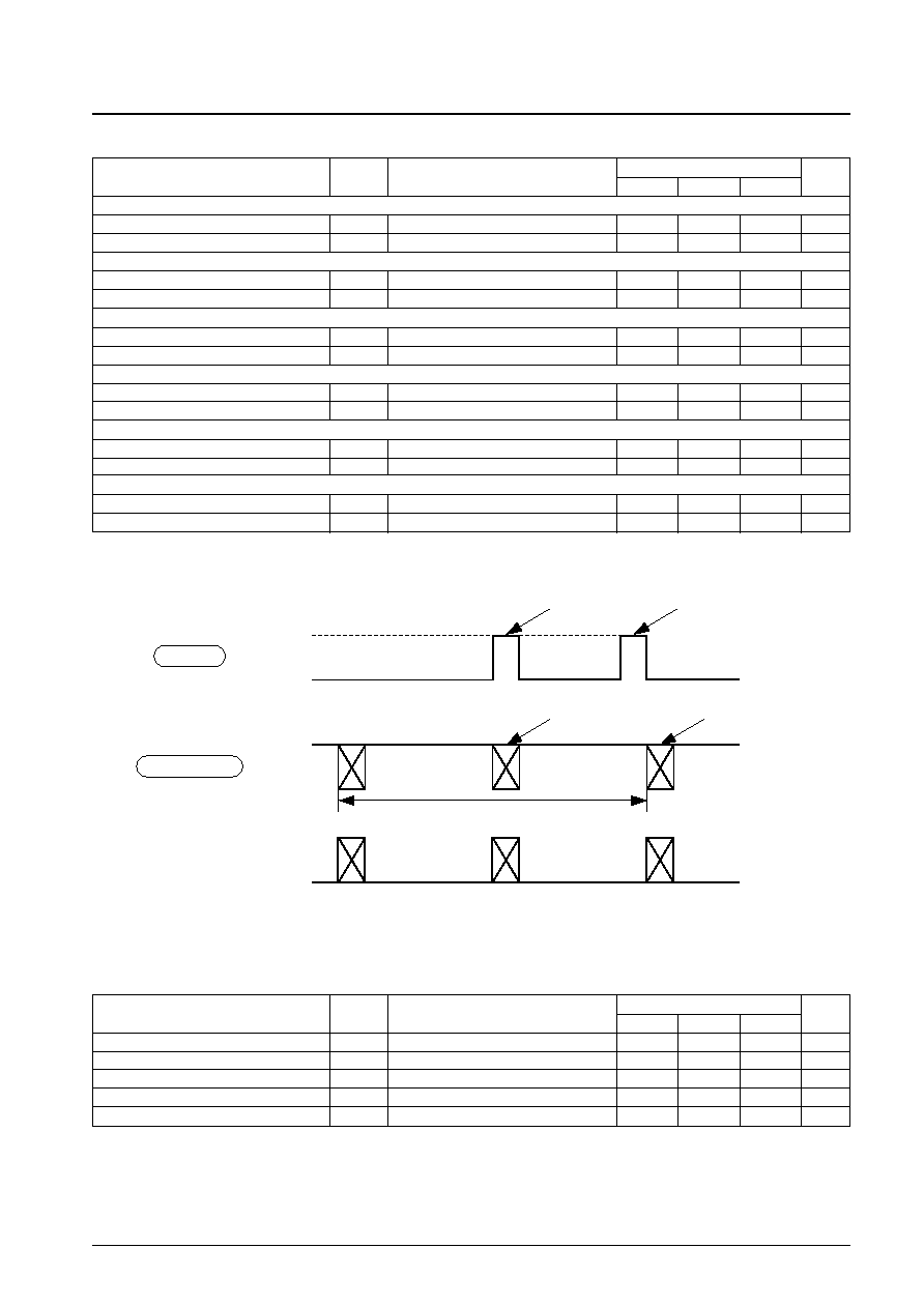
Note:
*
1 This must be adjusted so that image deterioration does not occur.
VHSUB
VLSUB
¯1
¯2, ¯3
¯NSUB
A12554
Imaging block pulses
Shutter pulse
*
2
Slice pulse
Charge sweep-out pulse
Frame shift
One field
Note:
*
2 If a shutter operation is performed when there is a signal in the storage block (that is, during signal readout), charge may be lost from the storage
block. Therefore, applications must not perform shutter operations with this timing.
Parameter
Symbol
Conditions
Ratings
Unit
min
typ
max
P well
V
PW
0
V
Output circuit voltage
V
DD
*
1
14.5
15.0
15.5
V
Output circuit voltage
V
GG
*
2
1.2
1.5
1.8
V
Reset drain
V
RD
12.5
13.0
13.5
V
OG bias
V
OG
*
2
3
3.5
4
V
Bias Conditions
Notes: 1. This level must never rise above the substrate pulse low level, V
LSUB
.
2. These input pins are high-impedance inputs.
No. 6247-5/9
LC99104
Parameter
Symbol
Conditions
Ratings
Unit
min
typ
max
DC operating current
I
DD
4.5
7.0
11.0
mA
DC Characteristics
Parameter
Symbol
Conditions
Ratings
Unit
min
typ
max
Sensitivity
S
Test procedure 1
200
mV
Image signal uniformity
VF
Test procedure 2
15
%
Saturated signal
Vsat
Test procedure 3
400
mV
Smear
SM
Test procedure 4
*
0.035
%
Dark signal
Vdark
Test procedure 5, Ta = 55∞C
14
mV
characteristics
1
--
Imaging Characteristics
(Storage time: 1/20 s) at Ta = 25∞C
Note:
*
When the frame shift frequency is 3.0 MHz, and when the storage time is 1/20 s.
Test Procedures
Use the standard drive conditions (see pages 3 and 4), the Sanyo evaluation unit, and the Advantest T8331 tester for the
following tests.
1. Sensitivity
Use the CCD-SY1 (manufactured by Wakasa Optical Institute, Ltd.) as the light source, and illuminate the surface of
the device to an intensity of 5 lux. Use the T8331 manufactured by Advantest to measure the CCD output from center
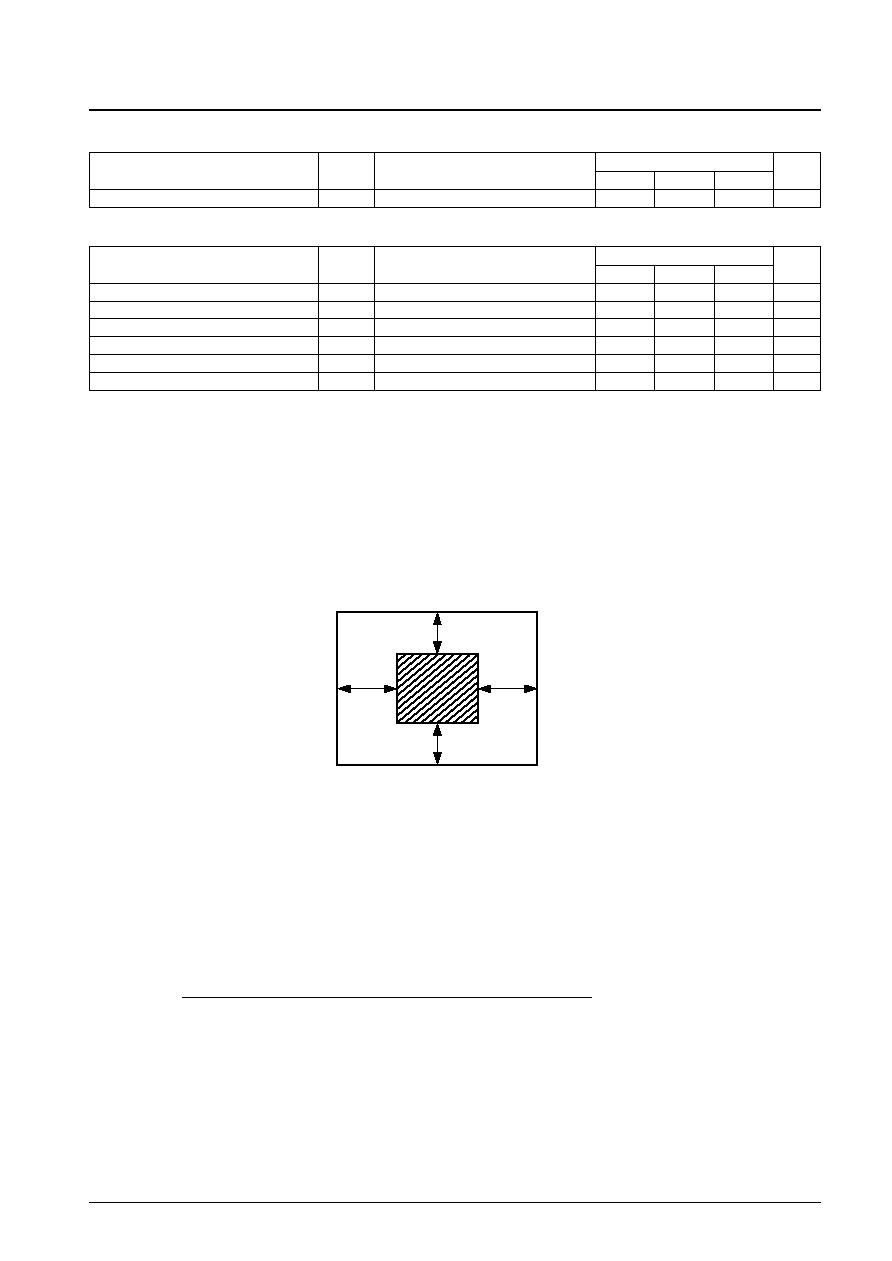
of the screen as shown in the figure below to determine the sensitivity.
H/4
V/4
A12555
H/4
V/4
2. Image signal uniformity
Perform this test under the following conditions.
∑ Standard drive conditions (See the device specifications.)
∑ Use a Halogen lamp with a color temperature of 3200 ∞K as the light source.
∑ Use a C-500 (1 mm thick) IR blocking filter.
Set the CCD surface illumination to 5 lux and divide the screen into 45 blocks as shown below. Measure the average
value for each block and determine the maximum, minimum, and mean values. Determine the ratio of the difference
(between the maximum and the minimum values) and the mean value.
VF =
Maximum of the block averages ≠ Minimum of the block averages
Mean of the block averages