Ordering number : ENN6246A
30300TH (OT)/30899TH (OT) No.6246-1/9
LC99160GL-TP
SANYO Electric Co.,Ltd. Semiconductor Company
TOKYO OFFICE Tokyo Bldg., 1-10, 1 Chome, Ueno, Taito-ku, TOKYO, 110-8534 JAPAN
1/4-Inch Optical Size ITU601 Format Compliant
Color Solid-State Image Sensor
Overview
The LC99160GL is a 1/4-inch optical size frame transfer
CCD solid state image sensor supporting ITU601 format .
In addition to interlace read-out, it enables all-pixel read-
out (progressive scan), in which signals from all-pixeles
can be read in one frame. Using with Sanyo's signal
processing IC LC99501, it provides NTSC, PAL, or VGA
format video signal.
Features
∑ Supports ITU601 format
∑ Interlace read-out/all-pixel read-out (progressive scan)
∑ Variable speed electronic shutter
Element Structure
∑ Number of effective pixels 736H
◊
490V
∑ Number of total pixels 780H
◊
510V
∑ Number of optical black pixels :
H direction : 32 pixels (front), 12 pixels (rear)
V direction : 8 pixels (above), 12 pixels (below)
∑ Dummy bit : 4 pixels (H front)
∑ Unit cell size : 5.00 µm (H)
◊
5.55 µm (V)
∑ Complementary color stripe filter (Ye, Cy, Mg)
∑ Parallel gate type CCD sensor
∑ Both imaging and storage areas are composed of 780H
◊
510V pixels
∑ 3-phase drive for imaging and storage areas,
2-phase drive for horizontal area
∑ Built-in high-sensitivity output amplifier
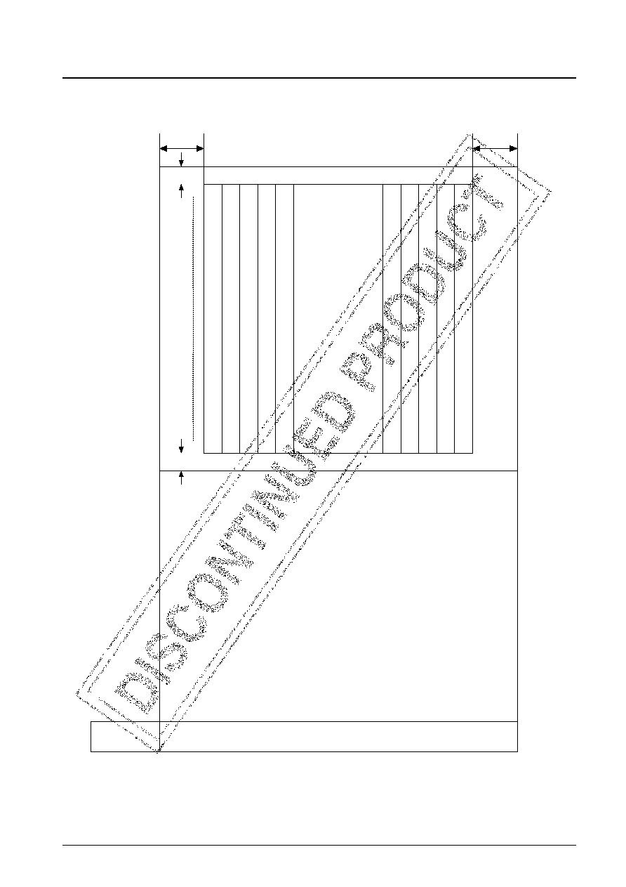
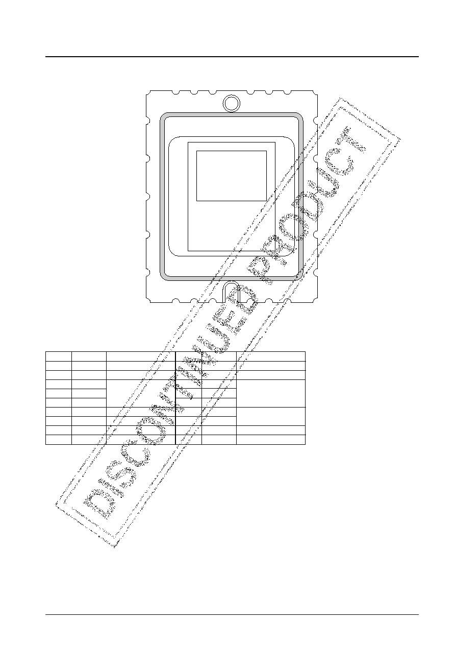
Package Dimensions
unit: mm
3242
11.8
10.16
0.7
2.54
1.0
7.62
R0.3
R0.25
1.49
1.05
0.44
0.635
1.075
2.0
Resin
Glass
Sensor
4.53
6.0
12.3
14.3
8.0
8.6
1.2
1.015
Optical Center
1.0
(1.2)
R1.0
(R0.6)
(R0.5)
[LC99160GL-TP]
Any and all SANYO products described or contained herein do not have specifications that can handle
applications that require extremely high levels of reliability, such as life-support systems, aircraft's
control systems, or other applications whose failure can be reasonably expected to result in serious
physical and/or material damage. Consult with your SANYO representative nearest you before using
any SANYO products described or contained herein in such applications.
SANYO assumes no responsibility for equipment failures that result from using products at values that
exceed, even momentarily, rated values (such as maximum ratings, operating condition ranges, or other
parameters) listed in products specifications of any and all SANYO products described or contained
herein.
No. 6246-2/9
LC99160GL-TP
Parameter
Symbol
Conditions
Ratings
Unit
Supply voltage
V
DD,
V
RD
V
PW
= 0 V
≠ 0.3 to + 15
V
Load gate voltage
V
GG
V
PW
= 0 V
≠ 0.3 to + 3
V
N-substrate-P-well voltage
NSUB-VPW, V
PW
= 0
≠ 0.3 to + 35
V
N-substrate-imaging block voltage
NSUB-PI1 to PI3, PS1 to PS3, V
PW
= 0 V
≠ 0.3 to + 35
V
Horizontal clock, reset gate voltage
Horizontal clock pin, PR, V
PW
= 0 V
≠ 0.3 to + 15
V
Clock voltage
Clock pins other than listed above, V
PW
= 0 V
≠ 15 to + 15
V
Pin voltage
Pins other than listed above
≠ 0.3 to + 10
V
Operating temperature
Topr
≠10 to +60
∞C
Storage temperature
Tstg
≠30 to +80
∞C
Specifications
Absolute Maximum Ratings
at Ta = 25∞C
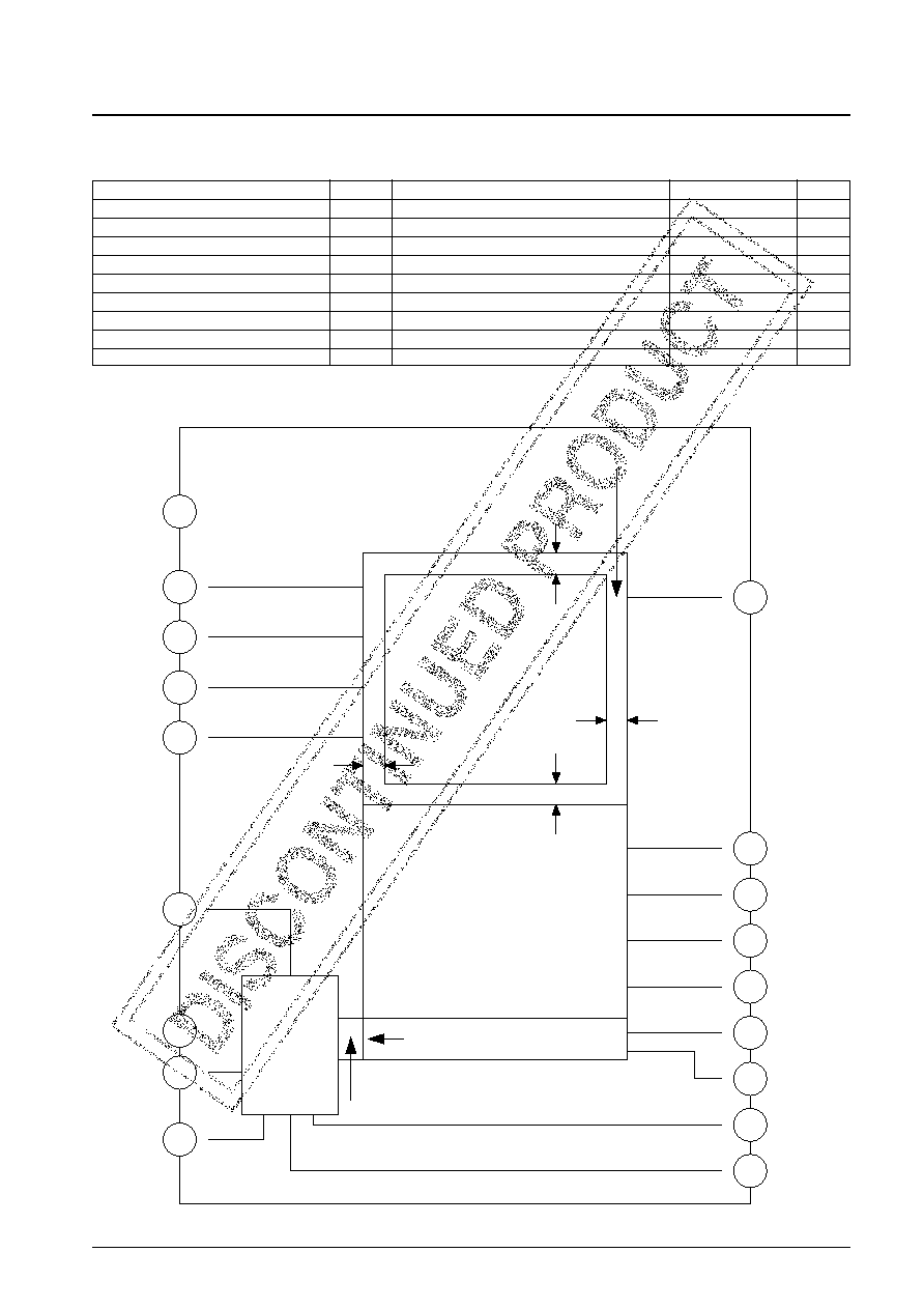
Block Diagram
1
VPW
2
NC
3
PI3
4
PI2
5
PI1
6
PR
7
VRD
8
VDD
9
VOUT
18
NSUB
17
NC
16
PS1
15
PS2
14
PS3
13
PH1
12
PH2
11
VOG
10
VGG
A12560
Optical black area
8 pixels
Imaging area
12 pixels
32 pixels
12 pixels
Storage area
Horizontal shift register (CCD)
4 dummy bits
Output Amplifire
No. 6246-5/9
LC99160GL-TP
Clock Voltage Conditions,
when the LC89901V CCD driver is used.
Parameter
Symbol
Conditions
Ratings
Unit
min
typ
max
Image area pulse signals
High level
V
PIF
PI1 to PI3
4.7
5.0
5.3
V
Low level
V
LIF
≠7.3
≠7.0
≠6.7
V
Storage area pulse signals
High level
V
PSL
PS1 to PS3
4.7
5.0
5.3
V
Low level
V
LSL
≠7.3
≠7.0
≠6.7
V
Horizontal transfer pulse signals
Pulse amplitude
V
PH
*
1 PH1, PH2
3.0
3.3
3.6
V
Low level
V
LH
PH1, PH2
0.0
0
0.5
V
Reset gate
Pulse amplitude
V
PR
PR
4.7
5.0
5.3
V
Low level
V
LR
*
2 PR
3.2
3.5
3.8
V
Substrate pulse signal
High level
V
HSUB
NSUB
19.5
20.0
20.5
V
Low level
V
LSUB
11.5
12.0
12.5
V
PI1
PI2
PI3
VHSUB
VLSUB
P-NSUB
A12563
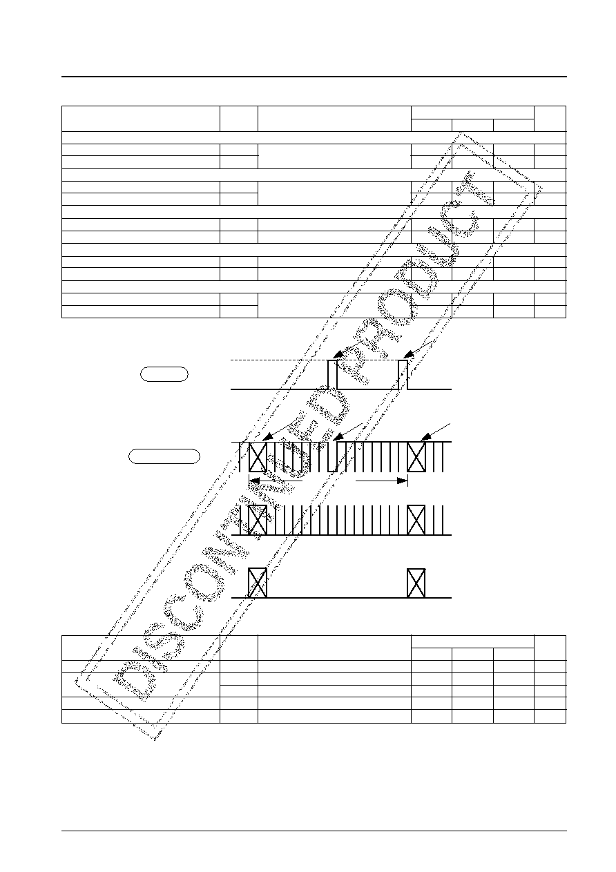
Image area pulse
Shutter pulse
Slice pulse
Frame shift
Charge sweep-out pulse
Frame shift
One field
Parameter
Symbol
Conditions
Ratings
Unit
min
typ
max
P well
V
PW
0
V
Output circuit voltage
V
DD
*
1
11.5
12.0
12.5
V
V
GG
*
2
1.7
2.0
2.3
V
Reset drain
V
RD
9.5
10.0
10.5
V
OG bias
V
OG
*
2
2.2
2.5
2.8
V
Bias Conditions
Notes: 1. The substrate pulse signal low level must not be higher than V
LSUB
.
2. These input pins are high-impedance inputs.