CMOS LSI
Ordering number : EN
*
5217
22896HA (OT) No. 5217-1/10
SANYO Electric Co.,Ltd. Semiconductor Bussiness Headquarters
TOKYO OFFICE Tokyo Bldg., 1-10, 1 Chome, Ueno, Taito-ku, TOKYO, 110-8534 JAPAN
1/6" Optical Size EIA B/W
Solid-State Image Sensor
LC9949G
Overview
The LC9949G is a 1/6" optical size frame transfer type
CCD (charge-coupled device) solid-state image sensor
developed for use in black-and-white video cameras.
Features
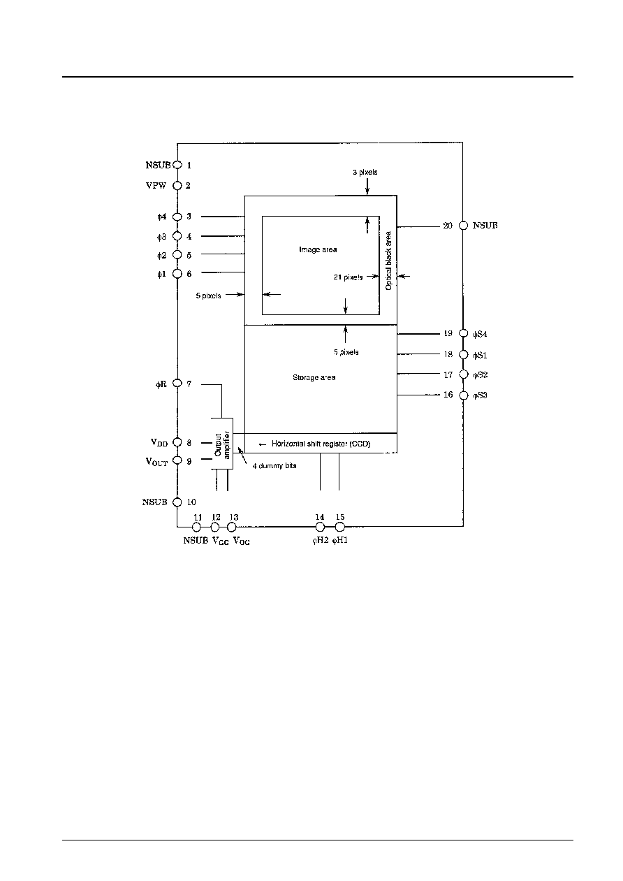
∑ Effective number of pixels (total pixels): 384H
◊
492V
(410H
◊
500V)
∑ Number of optical black pixels:
Horizontal direction: Front: 5 pixels
Back: 21 pixels
Vertical direction:
Front: 5 pixels
Back: 3 pixels
∑ Dummy bits: Horizontal direction: 4 pixels
∑ Horizontal resolution: 280 TV lines
∑ Supports miniature, compact camera designs.
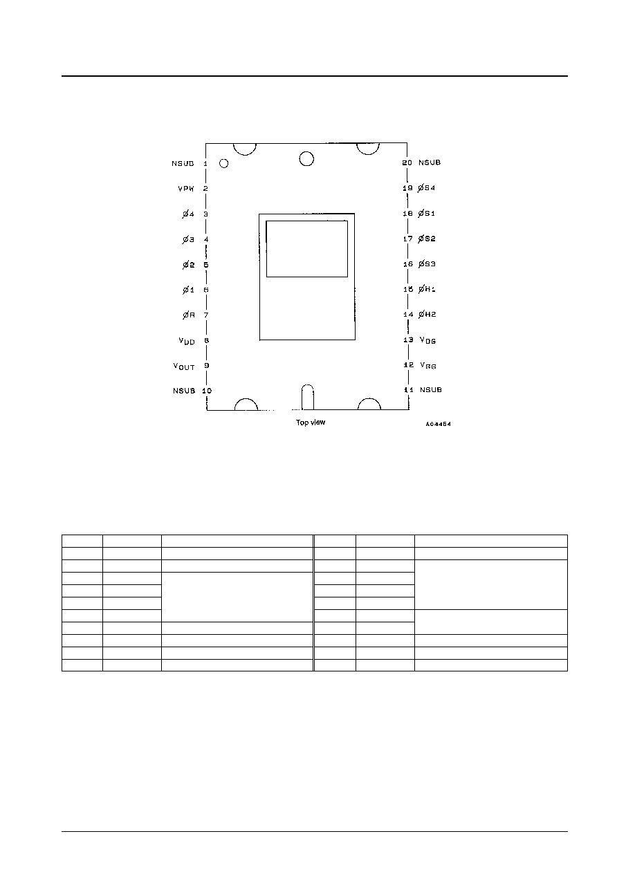
∑ Package: 20-pin half-pitch transparent DIP
∑ Horizontal shift register: 5 V drive
∑ Supports variable-speed electronic shutter operation
Device Structure
∑ 1/6" type frame transfer CCD image sensor
∑ Unit cell size: 6.5 Ķm (H)
◊
3.8 Ķm (V)
∑ Chip size: 3.79 mm (H)
◊
4.44 mm (V)
∑ Parallel gate CCD sensor
∑ Built-in high-sensitivity output amplifier
Specifications
Absolute Maximum Ratings
at Ta = 25įC
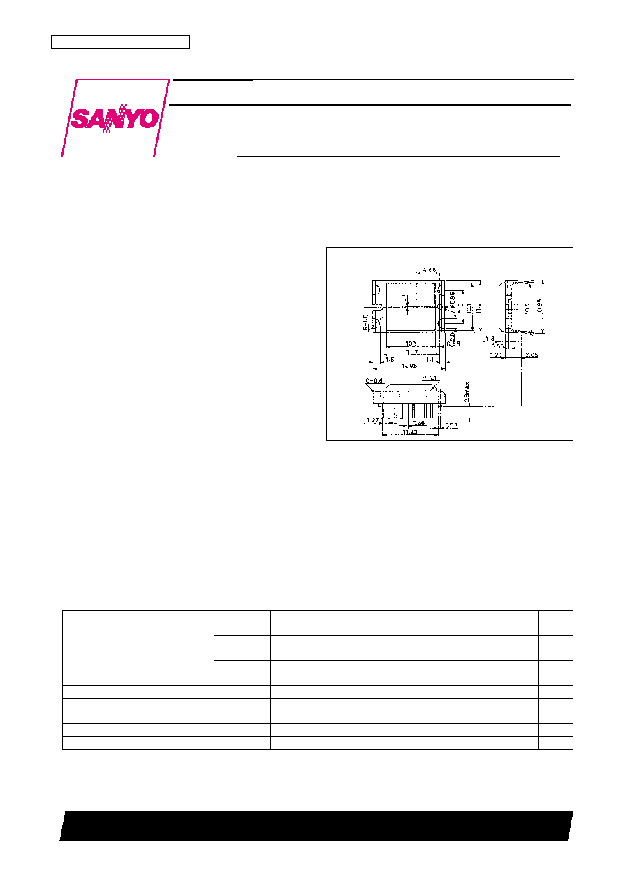
Package Dimensions
unit: mm
3218
Preliminary
[LC9949G]
Parameter
Symbol
Conditions
Ratings
Unit
V
DD
V
PW
= 0 V
≠0.3 to +18
V
V
GG
V
PW
= 0 V
≠0.3 to +5
V
Maximum supply voltage
NSUB-PW
≠0.3 to +50
V
NSUB - Ý1 to Ý4,
≠0.3 to +55
V
ÝS1 to ÝS4:
Horizontal clock pin
ÝR
V
PW
= 0 V
≠0.3 to +18
V
Other clock pins
V
PW
= 0 V
≠15 to +18
V
Other pins
V
PW
= 0 V
≠0.3 to +10
V
Operating temperature
Topr
≠10 to +60
įC
Storage temperature
Tstg
≠30 to +80
įC
Specifications
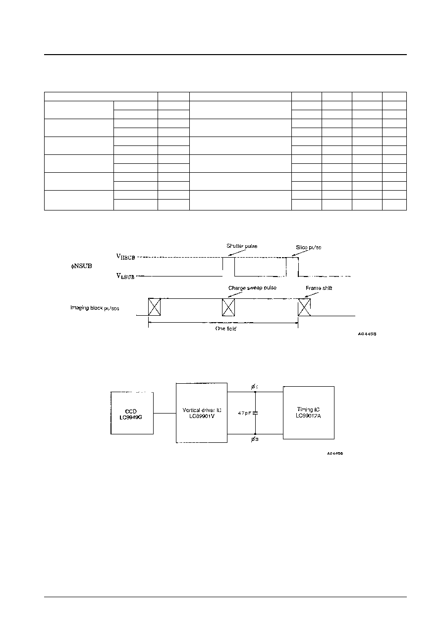
Clock Voltage Conditions
at Frame frequency = 3.58 MHz
Note: 1. Insert 47 pF capacitors as shown in Figure 2.
2. Adjust V
HSUB
within the range where image degradation does not occur so that the saturated output level is maximized.
Figure 1
Figure 2
No. 5217-4/10
LC9949G
Parameter
Symbol
Conditions
min
typ
max
Unit
Imaging block pulses
Pulse amplitude
V
PIF
*
1
14.0
14.5
15.0
V
Ý1, Ý2, Ý3, Ý4
Low level
V
LIF
≠10.0
≠9.5
≠9.0
V
Storage block pulses
Pulse amplitude
V
PSL
14.0
14.5
15.0
V
ÝS1, ÝS2
Low level
V
LSL
≠7.0
≠6.5
≠6.0
V
Storage block pulses
Pulse amplitude
V
PSL
14.0
14.5
15.0
V
ÝS3, ÝS4
Low level
V
LSL
≠8.0
≠7.5
≠7.0
V
Horizontal transfer pulses
Pulse amplitude
V
PH
4.5
5.0
5.5
V
ÝH1, ÝH2
Low level
V
LH
0
0
0.5
V
Reset gate
Pulse amplitude
V
PR
4.5
5.0
5.5
V
ÝR
Low level
V
LR
3.6
4.0
4.4
V
Substrate pulse
High level
V
HSUB
*
2
See Figure 1.
40.0
V
ÝNSUB
Low level
V
LSUB
17.5
18.0
18.5
V

Bias Conditions
Note: 1. Design applications so that this level never exceeds the substrate pulse low level VLSUB.
2. These are high-impedance inputs.
DC Characteristics
DC operating current
Note: VP: pulse amplitude
VL: low level
Figure 3 Pulse Waveform
No. 5217-5/10
LC9949G
Parameter
Symbol
Conditions
min
typ
max
Unit
P-well
V
PW
0
V
Output circuit voltage
V
DD
*
1
14.5
15.0
15.5
V
V
GG
*
2
0.5
0.8
1.1
V
OG bias
V
OG
*
2
4.5
5.0
5.5
V
Parameter
Symbol
Conditions
min
typ
max
Unit
DC operating current
I
DD
0.5
1.5
2.5
mA
Symbol
t
WH
t
WL
t
r
t
f
Conditions
Unit
typ
typ
typ
typ
Ý1
167
99
6.5
6.5
Ý2
146
120
6.5
6.5
During frame drive
ns
Ý3
167
99
6.5
6.5
When the frame shift frequency is 3.58 MHz
Ý4
146
120
6.5
6.5
ÝS1
146
120
6.5
6.5
ÝS2
146
120
6.5
6.5
During frame drive
ns
ÝS3
146
120
6.5
6.5
When the frame shift frequency is 3.58 MHz
ÝS4
146
120
6.5
6.5
ÝS1
1.36
62.1
30
30
ÝS2
1.36
62.1
30
30
The values enclosed in dark lines are in Ķs units and apply
ns
ÝS3
62.1
1.36
30
30
during 1H line transfers.
ÝS4
62.1
1.36
30
30
ÝR
29
104
3.5
3.5
Reset pulse
ÝH1
67
67
3
3
During horizontal transfers
ns
ÝH2
67
67
3
3
ÝNSUB
9.9
16.59
*
0.07
0.93
The slice pulse values marked
*
is in ms units.
Ķs
ÝNSUB
4.2
16.59
*
0.07
0.93
The shutter pulse values marked
*
is in ms units.
Ķs