LE25FV051T
3.3V-only 512k-Bit Serial Flash EEPROM
Preliminary Specifications
SANYO Electric Co., Ltd.
3/10
Command Definition
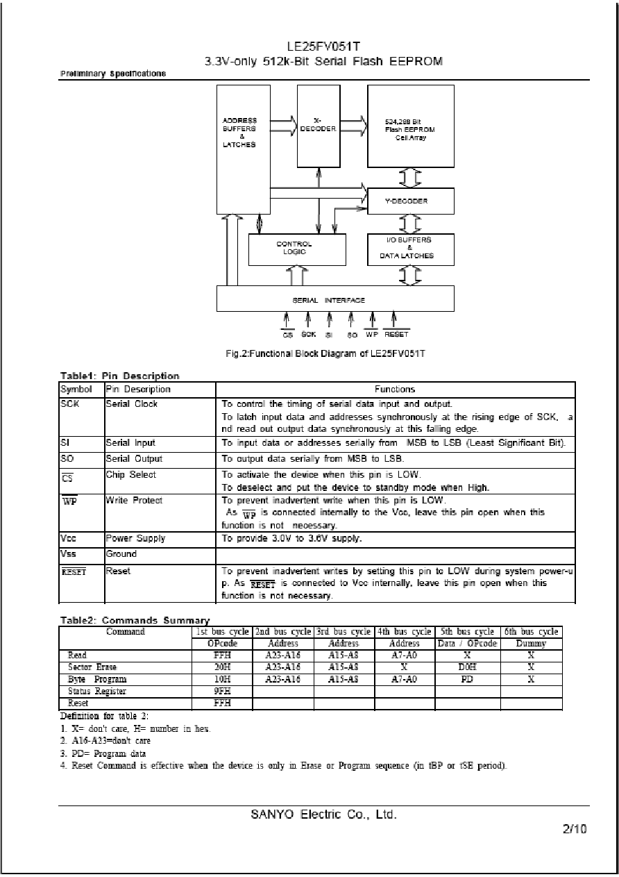
Table 2 contains a command list and a brief summary
of the commands. The following is a detailed description
of the options initiated by each command.
Read
Fig.5 shows the timing waveform of read operation.
The read operation is initiated by READ command. After
writing OPcode of "FFH" and following 24bit address and
16 dummy bits, SO is transformed into Low-impedance
state, and the specified addresses' data are read out
synchronously with SCK clock. While the SCK clock is
continuously on, the device counts up the next address
automatically and reads the data in order. When the
address reaches its maximum, while the read operation
still be continuing, the address is reset to the lowest one,
and the device continues reading data from the beginning.
When
CS
is set High so as to deselect the device,
the read operation terminates with the output in High-
impedance state. Do not execute read operation while the
device is in Byte_Program or Sector_Erase Cycle to
prevent inadvertent writes.
Status_Register Read
Fig.6 shows the timing waveform of Status_Register
Read.
Status_Register can be read while the device is in
Program or Erase mode. As is shown in the table below,
the LSB (Least Significant Bit) of Status_Register is set to
BSY
with other bits intact. By setting
CS
to LOW and
writing "9FH" in command register, the contents of the
Status_Register come out from MSB. The LSB of the
Status_Register stands for if the device is busy or not.
Therefore,"0" stands for busy and "1" for not in Program
or Erase mode. When
CS
goes High, Status Register
reading terminates with the output pin in High-
impedance state.
Sector_Erase
Fig.7 shows the timing waveform of Sector_Erase.
Sector_Erase command consists of 6 bus cycles from 1
st
bus cycle to 6
th
bus cycle. This command stages the
device for electrical erasing of all bytes within a sector. A
sector contains 256 bytes. This sector erasability
enhances the flexibility and usefulness of the
LE25FV051T
, since most applications only need to
change a small number of bytes or sectors, not the
entire chip. To execute the Sector_Erase operation, erase
address, 2
nd
OPcode (D0H) and Dummy bits must be
written to the command register after writing 1
st
OPcode
of (20H). This two-step sequence ensures that only
memory contents within the addressed sector are erased
and other sectors are not inadvertently erased. The erase
operation begins with the rising edge of the
CS
pulse and
terminates automatically by using an internal timer.
Termination of this mode is found out by using Status
Register Read.
Byte_Program
Fig.8 shows the timing waveform of Byte_Program.
Byte_Program command consists of 6 bus cycles from 1
st
bus cycle to 6
th
bus cycle, and stages the device for Byte
programmable. To execute the Byte_Program operation,
program address, program data and Dummy bits must be
written to the command register after writing the OPcode
of (10H). The program operation begins with the rising
edge of the
CS
pulse and terminates automatically by
using an internal timer. Termination of this mode is found
out by using Status Register Read.
Reset
Fig.9 shows the timing waveform of Reset operation.
Reset operation is effective while the device is already in
Program or Erase mode. But the data of specified
address are not guaranteed. The Reset Command can be
provided as a means to safely abort the Erase or Program
Command sequences. Following 4
th
bus cycles (erase or
program) with a write of (FFH) in 5
th
bus cycle will safely
abort the operation. Memory contents will not be altered.
Hardware Write Protection
Setting
WP
to LOW prevents inadvertent writes by
inhibiting write operation. As
WP
is connected internally
to the Vcc, don't connect externally to any nodes when
this function is not necessary. To prevent inadvertent
writes during system power-up, LE25FV051T has power-
on-reset circuit.
To perform power up more safely, the usage of
RESET
is recommended as follows. By holding
RESET
LOW during system power up and setting to High after
Vcc reaches operation voltage, inadvertent writes can be
prevented (see Fig.10). Don't use this function except
during power up. As
RESET
is connected to Vcc
internally, don't connect externally to any nodes when this
function is not
necessary
.
Decoupling Capacitors
Ceramic capacitors (0.1 µF) must be added between
V
CC
and V
SS
to each device to assure stable flash memory
operation.
7(MSB)
6
5
4
3
2
1
0(LSB)
X
X
X
X
X
X
X
BSY

LE25FV051T
3.3V-only 512k-Bit Serial Flash EEPROM
Preliminary Specifications
SANYO Electric Co., Ltd.
4/10
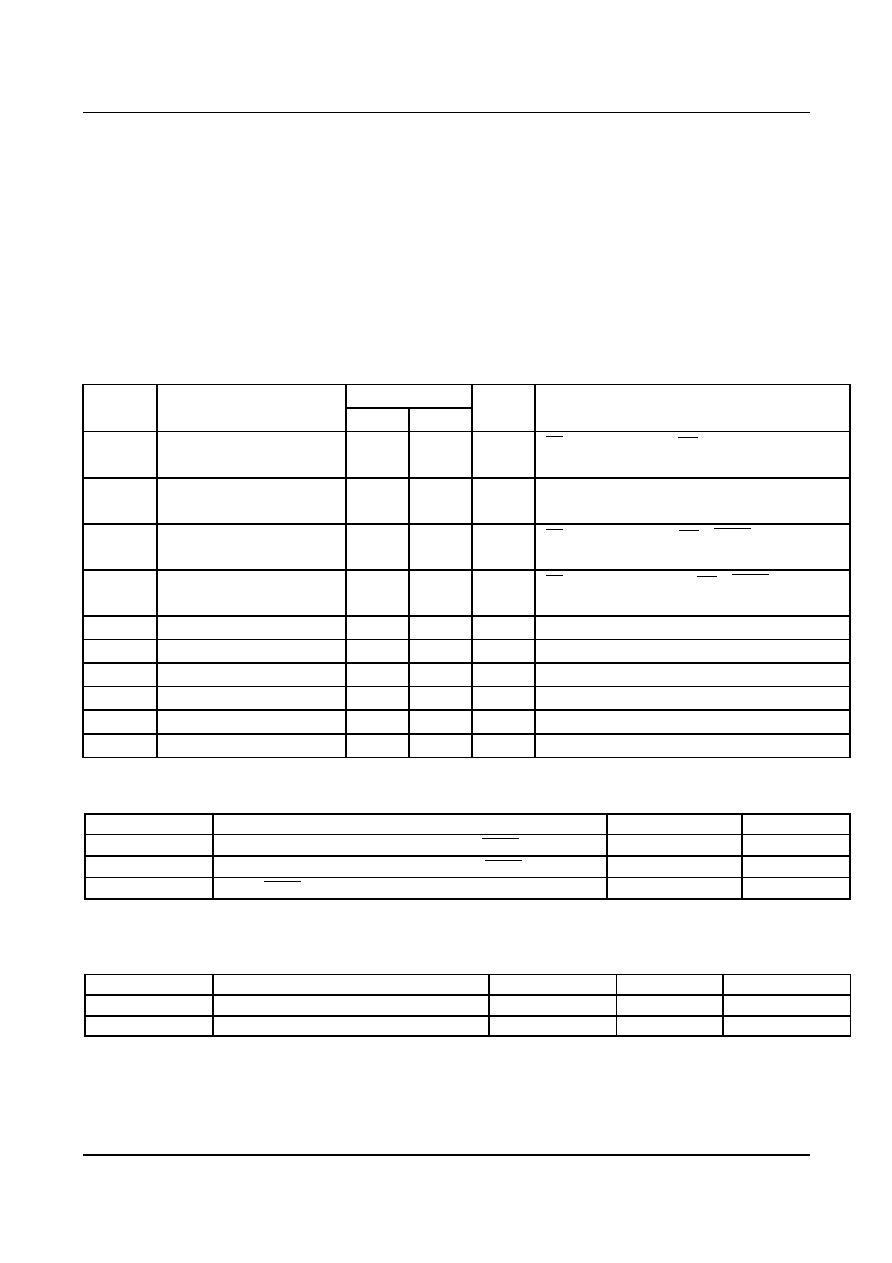
Absolute Maximum Stress Ratings
Storage Temperature........................................................-55 ∞C ~ 150 ∞C
Supply Voltage..................................................................-0.5 V ~ 4.6 V
D.C. Voltage on Any Pin to Grand Potential .....................-0.5 V ~ Vcc + 0.5 V
Permanent device damage may occur if ABSOLTE MAXIMUM RATINGS are exceeded.
Operating Range
Ambient Temperature .......................................................0 ∞C ~ 70 ∞C
Vcc ....................................................................................3.0 V ~ 3.6 V
DC Operating Characteristics
Symbol
Parameter
Limit
unit
Test Condition
Min.
Max.
ICCR
Power Supply Current
(Read)
10
mA
CS = VIL SO,
WP
open
SI = VIL / VIH, f = 10MHz, VCC = VCC max.
ICCW
Power Supply Current
(Write)
45
mA
VCC = VCC max.
ISB1
Standby Vcc Current
(TTL input)
3
mA
CS = VIH SO,
WP
,
RESET
open
VCC = VCC max.
ISB2
Standby Vcc Current
(CMOS input)
20
µA
CS = VCC≠0.3V SO,
WP
,
RESET
open
VCC = VCC max.
ILI
Input Leakage Current
10
µA
VIN = VSS ~ VCC, VCC = VCC max.
ILO
Output Leakage Current
10
µA
VIN = VSS ~ VCC, VCC = VCC max.
VIL
Input Low Voltage
≠0.3
0.4
V
VCC = VCC max.
VIH
Input High Voltage
2.4
Vcc+0.3
V
VCC = VCC min.
VOL
Output Low Voltage
0.2
V
IOL = 100 µA, VCC = VCC min.
VOH
Output High Voltage
Vcc-0.2
V
IOH = ≠100 µA, VCC = VCC min.
Power-up Timing
Symbol
Parameter
Minimum
Units
tPU_READ
Power-up to Read Operation(without using
RESET
)
10
ms
tPU_WRITE
Power-up to Write Operation(without using
RESET
)
10
ms
tPU_RST
From
RESET
goes High to Command Entry
1
µs
Capacitance (Ta = 25 ∞C, f = 1 MHz)
Symbol
Description
Maximum
Unit
Test Condition
CDQ
DQ Pin Capacitance
12
pF
VDQ = 0V
CIN
Input Capacitance
6
pF
VIN = 0V
Note: These parameters are periodically sampled and are not 100% tested.


