
Preliminary Specifications
CMOS LSI
LE28F4001CTS-12
4M-Bit (512k ◊ 8) Flash EEPROM
*This product incorporate technology licensed from Silicon Storage Technology, Inc.
This preliminary specification is subject to change without notice.
SANYO Electric Co., Ltd. Semiconductor Company
1-1, 1 Chome, Sakata, Oizumi-machi, Ora-gun, GUNMA, 370-0596 JAPAN
Revision 2.20-February 23,2001-AY/ay-1/14
Features
CMOS Flash EEPROM Technology
Single 5-Volt Read and Write Operations
Sector Erase Capability: 256 Bytes per sector
Fast Access Time: 120 ns
Low Power Consumption
Active Current(Read): 25 mA (Max.)
Standby Current: 20
µ
A (Max.)
High Read/Write Reliability
Sector-write Endurance Cycles: 10
4
10 Years Data Retention
Latched Address and Data
Self-timed Erase and Programming
Byte Programming: 40
µ
µ
µ
µ
s (Max.)
End of Write Detection:Toggle Bit/
DATA
Polling
Hardware/Software Data Protection
JEDEC Standard Byte-Wide EEPROM Pinouts
Packages Available
LE28F4001CTS: 32-pin TSOP Normal(8◊14mm)
Product Description
The LE28F4001C is a 512K
◊
8 CMOS sector erase, byte
program EEPROM. The LE28F4001C is manufactured
using SANYO's proprietary, high performance CMOS Flash
EEPROM technology. Breakthroughs in EEPROM cell
design and process architecture attain better reliability and
manufacturability compared with conventional approaches.
The LE28F4001C erases and programs with a 5-volt only
power supply. LE28F4001C conforms to JEDEC standard
pinouts for byte wide memories and is compatible with
existing industry standard EPROM, flash EPROM and
EEPROM pinouts.
Featuring high performance programming, the
LE28F4001C typically byte programs in 30
µ
s. The
LE28F4001C typically sector (256 bytes) erases in 2ms. Both
program and erase times can be optimized using interface
feature such as Toggle bit or
DATA
Polling to indicate the
completion of the write cycle. To protect against an
inadvertent write, the LE28F4001C has on chip hardware and
software date protection schemes. Designed, manufactured,
and tested for a wide spectrum of applications, the
LE28F4001C is offered with a guaranteed sector write
endurance of 10
4
cycles. Data retention is rated greater then
10 years.
The LE28F4001C is best suited for applications that
require reprogrammable nonvolatile mass storage of
program or data memory. For all system applications, the
LE28F4001C significantly improves performance and
reliability, while lowering power consumption when
compared with floppy diskettes or EPROM approaches.
EEPROM technology makes possible convenient and
economical updating of codes and control programs on-line.
The LE28F4001C improves flexibility, while lowering the
cost, of program and configuration storage applications.
Figure 1 shows the pin assignments for the 32 lead
Plastic TSOP packages. Figure 2 shows the functional block
diagram of the LE28F4001C. Pin description and operation
modes can be found in Tables 1 through 3.
Device Operation
Commands are used to initiate the memory operation
functions of the device. Commands are written to the device
using standard microprocessor write sequences. A command
is written by asserting
WE
low while keeping
CE
low.
The address bus is latched on the falling edge of
WE
,
CE
,
whichever occurs last. The data bus is latched on the rising
edge of
WE
,
CE
, whichever occurs first. However, during
the software write protection sequence the address are
latched on the rising edge of
OE
or
CE
, whichever occurs
first.

LE28F4001CTS-12
4M-Bit
Flash
EEPROM
Preliminary
Specifications
SANYO
Electric
Co.,
Ltd.
2/14
(Top View)
32 pin TSOP Normal
1
2
3
4
5
6
7
8
9
10
11
12
13
14
15
16
A11
A9
A8
A13
A14
A17
WE
Vcc
A18
A16
A15
A12
A7
A6
A5
A4
32
31
30
29
28
27
26
25
24
23
22
21
20
19
18
17
OE
A10
CE
DQ7
DQ6
DQ5
DQ4
DQ3
Vss
DQ2
DQ1
DQ0
A0
A1
A2
A3
Figure 1: Pin Assignments for 32-pin Plastic TSOP
DQ7-DQ0
ADDRESS
BUFFERS
&
LATCHES
X-
DECODER
4,194,304 Bit
SuperFlash EEPROM
Cell Array
Y-DECODER
I/O BUFFERS
&
DATA LATCHES
CONTROL
LOGIC
A18-A0
CE
OE
WE
Figure 2: Functional Block Diagram of LE28F4001C
LE28F4001CTS-12
4M-Bit
Flash
EEPROM
Preliminary
Specifications
SANYO
Electric
Co.,
Ltd.
3/14
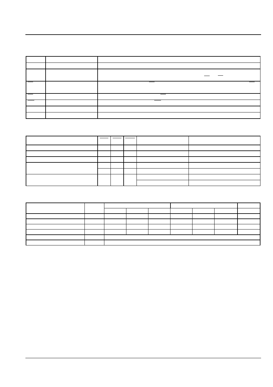
Table 1: Pin Description
Symbol
Pin
Name
Functions
A18-A0
Address Inputs
To provide memory address. Address are internally latched during write cycle.
DQ7-DQ0 Data Input/Output
To output data during read cycle and receive input data during write cycles. Data is internally
latched during a write cycle. The outputs are in tri-state when
OE
or CE is high.
CE
Chip Enable
To activate the device when CE is low. Deselects and puts the device to standby when CE is
high.
OE
Output Enable
To activate the data output buffers.
OE
is active low.
WE
Write Enable
To activate the write operation. WE is active low.
V
CC
Power Supply
To provide 5V
±
10% supply
.
V
SS
Ground
Table
2:
Operation
Modes
Selection
Mode
CE
OE
WE
DQ
Address
Read
V
IL
V
IL
V
IH
D
OUT
A
IN
Write
V
IL
V
IH
V
IL
D
IN
A
IN
Standby
V
IH
X
X
High-Z
X
Write Inhibit
X
V
IL
X
High-Z / D
OUT
X
X
X
V
IH
High-Z / D
OUT
X
Product ID
V
IL
V
IL
V
IH
Manufacturer Code (BF)
A18-A1=V
IL
, A9=12V, A0=V
IL
Device Code (04)
A18-A1=V
IL
, A9=12V, A0=V
IH
Table 3: Command Summary
Command
Required
Setup
Command
Cycle
Execute
Command
Cycle
SDP
Cycle
Operation
Address
Data
Operation
Address
Data
Sector_Erase
2
Write
X
20H
Write
SA
D0H
N
Byte_Program
2
Write
X
10H
Write
PA
PD
N
Reset 1
Write
X
FFH
Y
Read_ID
3
Write
X
90H
Read
(7)
(7)
Y
Software_Data_Unprotect (6)
7
Software_Data_Protect (6)
7
Definitions for Table 3:
1.
Type definitions : X=high or low
2.
Address definitions : SA=Sector Address=A18-A8 ; sector size=256byte ; A7-A0=X for this command
3.
Address definitions : PA=Program Address=A18-A0
4.
Data definition : PD=Program Data, H=number in hex.
5.
SDP=Software Data Protect mode using 7-Read-Cycle-Sequence.
Y=the operation can be executed with software data protect enabled. N=the operation cannot be executed with software data protect enabled.
6.
Refer to Figure 11 and 12 for the 7-Read-Cycle-Sequence Software Data Protection.
7.
Address 0000H retrieves the manufacturer code of BF(Hex), address 0001H retrieves the device code of 04(Hex).

LE28F4001CTS-12
4M-Bit
Flash
EEPROM
Preliminary
Specifications
SANYO
Electric
Co.,
Ltd.
4/14
Command Definition
Table 3 contains a command list and a brief summary of the
commands.
The following is a detailed description of the options initiated
by each command.
The LE28F4001C has to have the Software Data Unprotect
Sequence executed prior a Byte Program or Erase in order to
perform those functions.
Sector_Erase Operation
The Sector_Erase operation is initiated by a setup command
and an execute command. The setup command stages the device
for electrical erasing of all bytes within a sector. A sector contains
256 bytes. This sector erasability enhances the flexibility and
usefulness of the LE28F4001C, since most applications only need
to change a small number of bytes or sectors, not the entire chip.
The setup command is performed by writing (20H) to the device.
To execute the sector-erase operation, the execute command (D0H)
must be written to the device. The erase operation begins with the
rising edge of the WE pulse and terminated automatically by
using an internal timer. See Figure 8 for timing waveforms.
The two-step sequence of a setup command followed by an
execute command ensures that only memory contents within the
addressed sector are erased and other sectors are not inadvertently
erased.
Sector_Erase Flowchart Description
Fast and Reliable erasing of the memory contents within a
sector is accomplished by following the sector erase flowchart as
shown in Figure 3. The entire procedure consists of the execution
of two commands. The Sector_Erase operation will terminate after
a maximum of 4ms. A Reset command can be executed to
terminate the erase operation; however, if the erase operation is
terminated prior to the 4ms time-out, the sector may not be
completely erased. An erase command can be reissued as many
times an necessary to complete the erase operation. The
LE28F4001C cannot be "overerased".
Byte_Program Operation
The Byte_Program operation is initiated by writing the setup
command (10H).
Once the program setup is performed, programming is executed
by the next WE pulse. See Figure 6 and 7 for timing waveforms.
The address bus is latched on the falling edge of WE , CE , or
the rising edge of
OE
, whichever occurs first. The programming
operation begins with either the rising edge of WE , CE ,
whichever occurs first. The programming operation is terminated
automatically by an internal timer. See the programming
characteristics and waveforms for details, Figures 4, 6 and 7.
The two-step sequence of a setup command followed by an
execute command ensures that only the addressed byte is
programmed and other bytes are not inadvertently programmed.
The Byte_Program Flow Chart Description
Programming data into the device is accomplished by following
the Byte_Program flowchart as shown in Figure 3. The
Byte_Program command sets up the byte for programming. The
address bus is latched on the falling edge of WE , CE ,
whichever occurs last. The data bus is latched on the rising edge of
WE , CE , whichever occurs first, and begins the program
operation. The end of write can be detected using either the
DATA
polling or Toggle bit.
Reset Operation
A Reset Command is provided as a means to safely abort the
erase or program command sequences. Following either setup
command (erase or program) with a write of (FFH) will safely
abort the operation. Memory contents will not be altered. After the
Reset command, the device returns to the read mode. The reset
command dose not enable write protect. See figure 10 for timing
waveforms.
Read Operation
The read operation is initiated by setting CE ,
OE
and WE
into the read mode. See Figure 5 for read memory timing
waveforms and Table 2 for the read mode. Read cycles from the
host retrieve data from the array. The device remains enabled for
read until another operating mode is accessed.
During initial power-up, the device is in the read mode and is
write protected. The device must be unprotected in order to execute
a write operation
The read operation is controlled by
OE
and CE at logic low.
When CE is high, the chip is deselected and only standby power
will be consumed.
OE
is the output control and is used to gate to
the output pins. The data bus is in a high impedance state when
either CE or
OE
is high.

LE28F4001CTS-12
4M-Bit
Flash
EEPROM
Preliminary
Specifications
SANYO
Electric
Co.,
Ltd.
5/14
Read_ID Operation
The Read_ID operation is initiated by writing a single
command (90H). A read of address 0000H will outputs the
manufacturer's code (BFH). A read of address 0001H will outputs
the device code (04H).Any other valid command will terminate this
operation.
Data Protection from Inadvertent Writes
In order to protect the integrity of nonvolatile data storage, the
LE28F4001C provides hardware and software features to prevent
writes to the device, for example, during system power-up or
power-down. Such provisions are described below.
Hardware Write Protection
The LE28F4001C is designed with hardware features to
prevent inadvertent writes. This is done in the following ways:
1. Write Inhibit Mode:
OE
low, CE high or WE high
inhibit the write operation.
2. Noise and Glitch Protection: Write operations are initiated
when the WE pulse width is less than 15 ns.
3. After power-up the device is in the read mode and the
device is in the write protect state.
Software Data Protection
Provisions have been made to further prevent inadvertent writes
through software. In order to perform the write functions of erase
or program, a two-step command sequence consisting of a setup
command followed by an execute command avoids inadvertent
erasing or programming of the device.
The LE28F4001C will default to write protect after power-up.
A sequence of seven consecutive reads at specified device
addresses will unprotect the device. The address sequence is
1823H, 1820H, 1822H, 0418H, 041BH, 0419H, 041AH. The
address has to be latched in the rising edge of
OE
or CE ,
whichever occurs first. A similar seven read sequence of 1823H,
1820H, 1822H, 0418H, 041BH, 0419H, 040AH will protect the
device. Also, refer to Figure 11, 12 for the 7-read-sequence
Software Write Protection. The DQ pins can be in any state (i.e.,
high, low, or High-Z).
End of Write Detection
Detection of where a write cycle ended is necessary to optimize
system performance. The end of a write cycle (erase or program)
can be detected by three means: 1) monitoring the
DATA
polling
bit; 2) monitoring the Toggle bit; 3) by two successive reads of the
same data. These three detection mechanisms are described below.
DATA
Polling (DQ7)
The LE28F4001C features
DATA
Polling to indicate the and
of a write cycle. During a write cycle, any attempt to read the last
byte loaded will result in the complement of the loaded data on
DQ7. Once the write cycle is completed, DQ7 will show true data.
See Figure 13 for timing waveforms. In order for
DATA
Polling
to function correctly, the byte being polled must be erased prior to
programming.
Toggle Bit (DQ6)
An alternate means for determining the end of a write cycle is
by monitoring the Toggle Bit DQ6. During a write operation,
successive attempts to read data from the device will result in DQ6
toggling between logic "1" (high) and "0" (low). Once the write
cycle has completed, DQ6 will stop toggling and valid data will be
read. The Toggle Bit may be monitored any time during the write
cycle. See Figure 14 for timing waveforms.
Successive Reads
An alternate means for determining the end of a write cycle is
by reading the same address for two consecutive data matches.
Product Identification
The Product Identification mode identifies the device and
manufacturer as SANYO. This mode may be accessed by hardware
or software operations. The hardware operation is typically used by
an external programming to identify the correct algorithm for the
SANYO LE28F4001C. Users may wish to use the software
operation to identify the device (i.e., using the device code). For
details, see Table 2 for the hardware operation. The manufacturer
and device codes are the same for both operations.
Notes for Operation
During power up, the device's state should be the write
inhibition mode. (During power up, the device's state should be
CE =V
IH
or
OE
=V
IL
or WE =V
IH
)
If CE = WE =V
IL
and
OE
=V
IH
during power up, RESET
command should be asserted before operation.