
Ordering number : EN
*
5239A
63096HA (OT) No. 5239-1/14
Overview
The LE28F4001 Series ICs are 524288-word
◊
8-bit flash
memory products that support on-board reprogramming
and feature 5 V single-voltage power supply operation.
CMOS peripheral circuits were adopted for high speed,
low power, and ease of use. These products support a
sector (256 bytes) erase function for fast data rewriting.
Features
∑ Fabricated in a highly reliable 2-layer polysilicon
CMOS flash EEPROM process.
∑ Read and write operation from a 5 V single-voltage
power supply
∑ Sector erase function: 256 bytes per sector
∑ Fast access time: 150/200 ns
∑ Low power
-- Operating current (read): 25 mA (maximum)
-- Standby current: 20 µA (maximum)
∑ Highly reliable read and write operations
-- Sector write cycles: 10
4
cycles
-- Data retention time: 10 years
∑ Address and data latches
∑ Self-timer erase and programming
∑ Byte programming time: 35 µs (maximum)
∑ Write complete detection: Toggle bit and data polling
∑ Hardware and software data protection
∑ Pin assignment conforms to the JEDEC byte-wide
EEPROM standard
∑ Packages
SOP 32-pin
(525 mil) plastic package
:LE28F4001M
TSOP 40-pin (10
◊
14 mm) plastic package :LE28F4001T
TSOP 40-pin (10
◊
14 mm) plastic package :LE28F4001R
Package Dimensions
unit: mm
3205-SOP32
unit: mm
3087A-TSOP40
Preliminary
SANYO: SOP32
[LE28F4001M]
SANYO: TSOP40 (TYPE-I)
[LE28F4001T, R]
LE28F4001M, T, R-15/20
SANYO Electric Co.,Ltd. Semiconductor Bussiness Headquarters
TOKYO OFFICE Tokyo Bldg., 1-10, 1 Chome, Ueno, Taito-ku, TOKYO, 110-8534 JAPAN
4 MEG (524288 words
◊
8 bits) Flash Memory
CMOS LSI
These FLASH MEMORY products incorporate technology licensed Silicon Storage Technology, Inc.
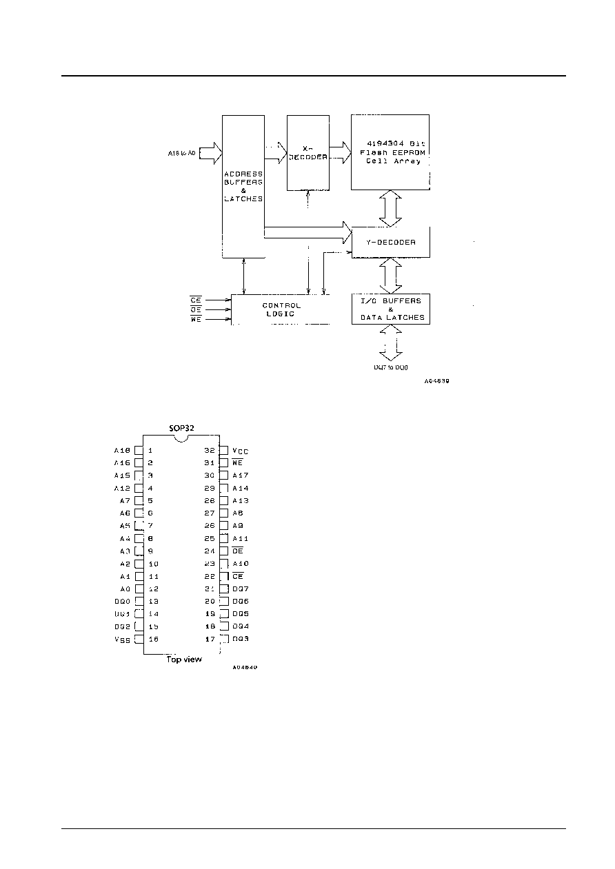
Block Diagram
Pin Assignments
No. 5239-2/14
LE28F4001M, T, R-15/20
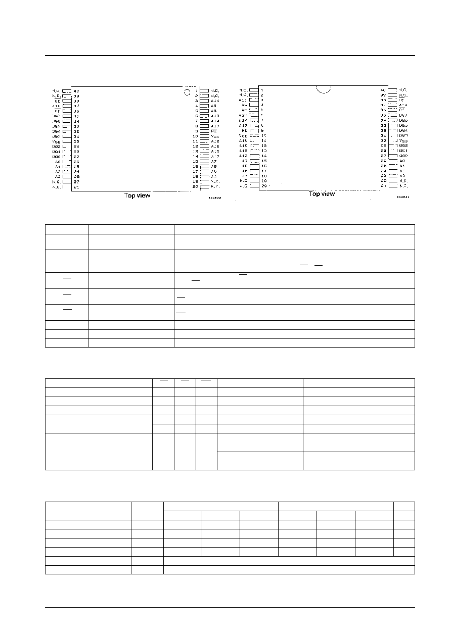
TSOP40 Standard
TSOP40 Reversed
Pin Functions
Function Logic
Command Settings
No. 5239-3/14
LE28F4001M, T, R-15/20
Symbol
Pin
Functions
A18 to A0
Address input
Supply the memory address to these pins.
The address is latched internally during a write cycle.
These pins output data during a read cycle and input data during a write cycle.
DQ7 to DQ0
Data input and output
Data is latched internally during a write cycle.
Outputs go to the high-impedance state when either OE or CE is high.
CE
Chip enable
The device is active when CE is low.
When CE is high, the device becomes unselected and goes to the standby state.
OE
Output enable
Makes the data output buffers active.
OE is a low-active input.
WE
Write enable
Makes the write operation active.
WE is a low-active input.
V
CC
Power supply
Apply 5 V (±10%) to this pin.
V
SS
Ground
N.C.
No connection
These pins must be left open.
Mode
CE
OE
WE
A18 to A0
DQ7 to DQ0
Read
V
IL
V
IL
V
IH
A
IN
D
OUT
Write
V
IL
V
IH
V
IL
A
IN
D
IN
Standby or write inhibit
V
IH
X
X
X
High-Z
Write inhibit
X
V
IL
X
X
High-Z/D
OUT
X
X
V
IH
X
High-Z/D
OUT
A18 to A10 = V
IL
, A8 to A1 = V
IL,
Manufacturer code (BF)
Product identification
V
IL
V
IL
V
IH
A9 = 12 V, A0 = V
IL
A18 to A10 = V
IL
, A8 to A1 = V
IL
Device code (04)
A9 = 12 V, A0 = V
IH
Command
Request
Setup command cycle
Execute command cycle
SDP
cycle
Operation
Address
Data
Operation
Address
Data
Sector erase
2
Write
X
20H
Write
SA
D0H
N
Byte program
2
Write
X
10H
Write
PA
PD
N
Reset
1
Write
X
FFH
Y
Read ID
3
Write
X
90H
Read
(7)
(7)
Y
Software data unprotect
7
See Figure 9.
Software data protect
7
See Figure 10.

Notes on Command Settings
1. Type definitions: X = Don't care
2. Address definitions: SA = Sector Address = A18 to A8; sector size = 256 bytes; A7 to A0 = X for this command.
3. Address definitions: PA = Program Address = A18 to A0.
4. Data definition: PD = Program Data, H = number in hex.
5. SDP = Software Data Protect mode using 7-read-cycle sequence.
Y = the operation can be executed with software data protect enabled. N = the operation cannot be executed with
software data protect enabled.
6. Refer to figures 9 and 10 for the 7-read-cycle sequence software data protection.
7. Address 0000H retrieves the manufacturer code of BF (hex), address 0001H retrieves the device code of 04 (hex).
Product Overview
The LE28F4001 Series products are EEPROMs that support sector erase and byte programming functions and that
feature a 512K
◊
8 organization. These products support both erase and programming from a 5-V single-voltage power
supply, conform to the JEDEC standards for byte-wide memory pin assignments, and are pin compatible with industry
standard EPROMs, flash EPROMs, and EEPROMs.
The LE28F4001 Series products, provide a 35 µs maximum byte programming time and a 4 ms sector erase time.
Programming and erase operations can both be optimized by using the toggle bit and Data polling functions that indicate
the completion of the write cycle. To protect data against unintentional writes, these products provide both hardware and
software data protection schemes. The LE28F4001 Series products, guarantee 10
4
sector write cycles. The data retention
time is ten years or longer.
The LE28F4001 Series functional block diagram and the 40-pin TSOP and 32-pin SOP package pin assignments are
shown on page 2, and the pin functions and command settings are listed on page 3.
Device Operation
Commands are used to execute the device's memory functions. Commands are written to the command register with
standard microprocessor write timing. Commands are written by setting WE low while CE is held low. The address is
latched on the falling edge of either CE or WE, whichever occurs later. Data is latched on the rising edge of either CE or
WE, whichever occurs first. However, the address is latched on the rising edge of either OE or CE, whichever occurs
first during the software write protect sequence.
Command Definition
The "Command Settings" section provided an overview and list of the LE28F4001 commands. This section describes the
functions provided by those commands in detail.
Before executing the LE28F4001 Series byte programming or erase functions, the application system must execute the
software data unprotect sequence.
No. 5239-4/14
LE28F4001M, T, R-15/20

1. Sector erase operation
The sector erase operation consists of a setup command and an execute command. The setup commands sets the
device to a state where all the bytes in the sector can be erased electrically. A single sector has 256 bytes. Since
almost all applications use erase operations that are not whole-chip erase operations but rather are single sector erase
operations, this sector erase function significantly increases the flexibility and ease of use of the LE28F4001 Series.
The setup command is executed by writing 20H to the command register.
An execute command (D0H) must be written to the command register to execute the sector erase operation. The
sector erase operation starts on the rising edge of the WE pulse and is automatically completed under internal timing
control. Figure 6 shows the timing waveforms for this operation.
This two stage sequence in which a setup command and a following execute command are required guarantees that
the memory at the sector specified by the address data will not be erased accidentally.
2. Sector erase flowchart
The quick and reliable erasure of up to 256 bytes of memory can be achieved by following the sector erase flowchart
shown in Figure 1. The whole operation consists of executing two commands. A sector erase operation completes in
a maximum of 4 ms. Although the erase operation can be completed by executing a reset operation, the sector may
not be completely erased if that reset is executed before the 4 ms time out period elapses. The erase command can be
re-executed as many times as required before the erase completes. Excessive erasure cannot cause problems with the
LE28F4001 Series products.
3. Byte programming operation
The byte programming operation is started by writing a setup command (10H) to the command register.
Once the setup command is executed, the execute command is started by the next WE pulse transition. Figure 7
shows the timing waveforms for this operation. The address and the data are latched internally on the falling edge
and rising edge of the WE pulse, respectively. The WE rising edge also corresponds to the start of the programming
operation. The programming operation is automatically completed under internal timing control. Figures 2 and 7
show the programming characteristics and waveforms.
As mentioned previously, this two stage sequence in which a setup command and a following execute operation are
required guarantees that the memory cells will not be programmed accidentally.
4. Byte programming flowchart
Figure 2 shows the device data programming operation. This is effected by following the byte programming
flowchart. The byte programming command sets up the byte to be written. The address is latched on the falling edge
of WE or CE, whichever is later. The data bus is latched on the rising edge of WE or CE, whichever is earlier, and
the programming operation starts at that point. The completion of the write operation can be detected using either the
toggle bit or by polling a Data pin.
5. Reset operation
The reset command is a procedure for safely terminating an erase or programming command sequence. Writing FFH
to the command register after issuing an erase or programming setup command will safely cancel that operation. The
contents of memory will not be changed. The device goes to read mode after executing a reset command. The reset
command cannot activate the software data protect function. Figure 8 shows the timing waveforms.
6. Read operation
A read operation is performed by setting CE and OE, and then WE, to read mode. Figure 3 shows the read mode
timing waveforms, and the read mode conditions are shown as "functional logic". A read cycle from the host
searches for the memory array data. The device remains in the read state until another command is written to the
command register.
As a default, the device will be in read mode in the write protect state from the time power is first applied until a
command is written to the command register. The unprotect sequence must be executed to perform a write operation
(erase or programming).
The read operation is controlled by CE and OE, and both must be set to the logic low level to activate the read
function. When CE is at the logic high level, the chip is in the unselected state and only draws the standby current.
OE controls the output pins. The device output pins will be in the high-impedance state if either CE or OE is at the
logic high level.
No. 5239-5/14
LE28F4001M, T, R-15/20