 | –≠–ª–µ–∫—Ç—Ä–æ–Ω–Ω—ã–π –∫–æ–º–ø–æ–Ω–µ–Ω—Ç: LM7001 | –°–∫–∞—á–∞—Ç—å:  PDF PDF  ZIP ZIP |
Ordering number : EN5262
D3095HA (OT) No. 5262-1/8
Features
∑ The LM7001J and LM7001JM are PLL frequency
synthesizer LSIs for tuners, making it possible to make
up high-performance AM/FM tuners easily.
∑ These LSIs are software compatible with the LM7000,
but do not include an IF calculation circuit.
∑ The FM VCO circuit includes a high-speed
programmable divider that can divide directly.
∑ Seven reference frequencies: 1, 5, 9, 10, 25, 50, and
100 kHz
∑ Band-switching outputs (3 bits)
∑ Controller clock output (400 kHz)
∑ Clock time base output (8 Hz)
∑ Serial input circuit for data input (using the CE, CL, and
DATA pins)
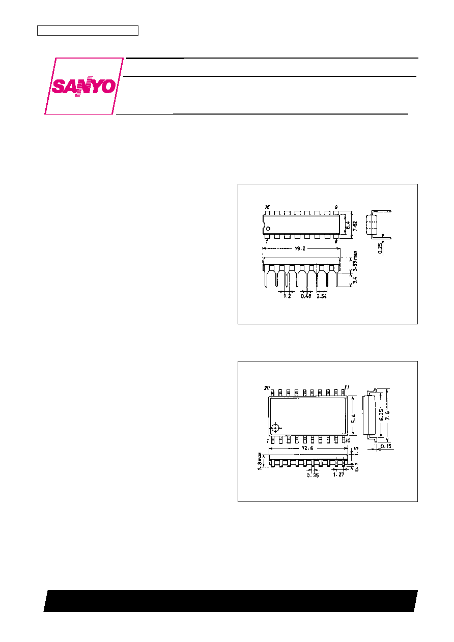
Package Dimensions
unit: mm
3006B-DIP16
unit: mm
3036B-MFP20
SANYO: DIP16
[LM7001J]
SANYO: MFP20
[LM7001JM]
LM7001J, 7001JM
SANYO Electric Co.,Ltd. Semiconductor Bussiness Headquarters
TOKYO OFFICE Tokyo Bldg., 1-10, 1 Chome, Ueno, Taito-ku, TOKYO, 110-8534 JAPAN
Direct PLL Frequency Synthesizers
for Electronic Tuning
NMOS LSI
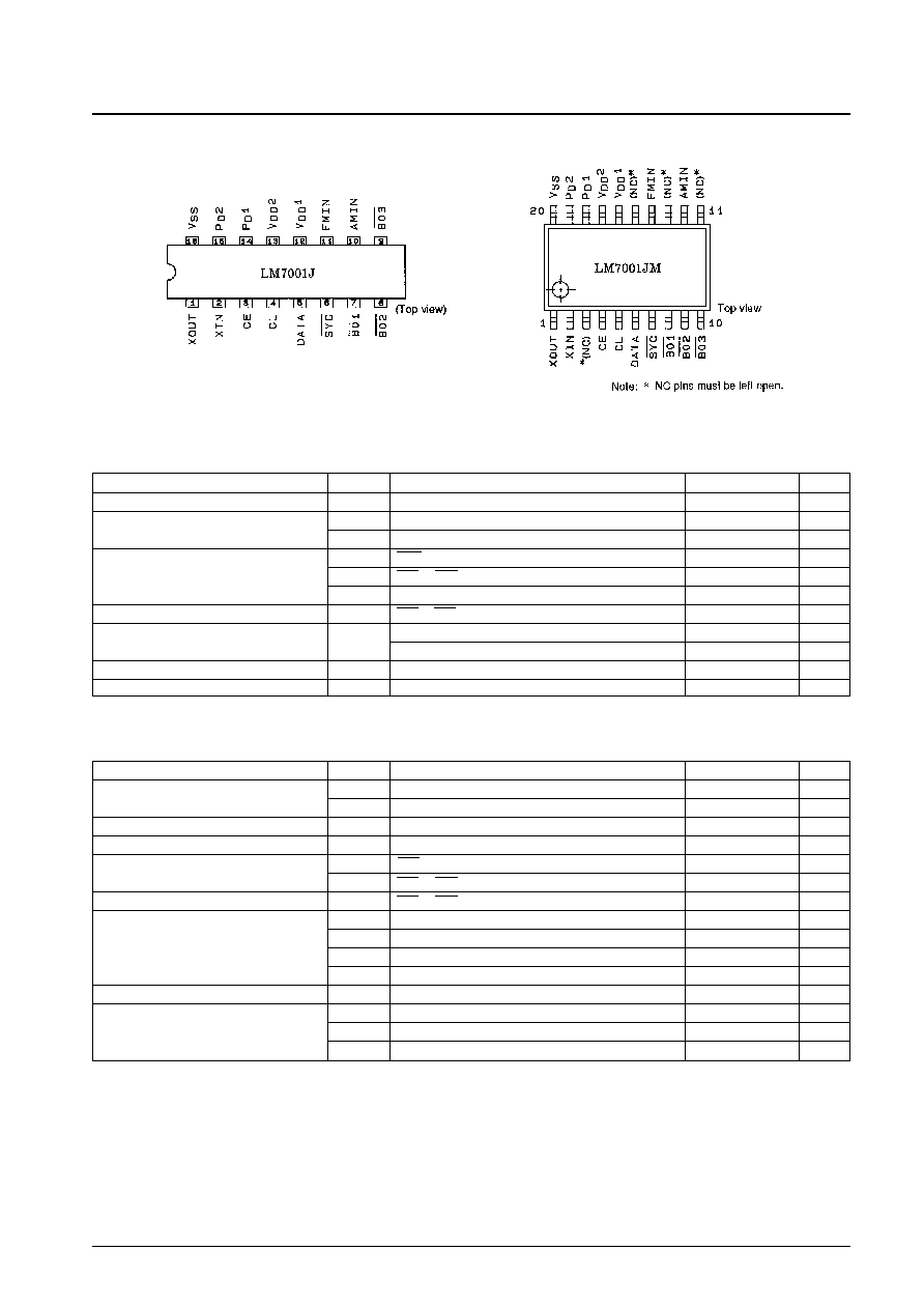
Pin Assignments
Specifications
Absolute Maximum Ratings
at Ta = 25∞C, V
SS
= 0 V
Allowable Operating Ranges
at Ta = ≠40 to +85∞C, V
SS
= 0 V
Note: 1. f
ref
= 25, 50, or 100 kHz
2. f
ref
= Reference frequencies other than those for
*
1.
3. "s" refers to the control bit in the serial data.
No. 5262-2/8
LM7001J, 7001JM
Parameter
Symbol
Conditions
Ratings
Unit
Maximum supply voltage
V
DD
max
V
DD
1, V
DD
2
≠0.3 to +7.0
V
Maximum input voltage
V
IN
1 max
CE, CL, DATA
≠0.3 to +7.0
V
V
IN
2 max
Input pins other than V
IN
1
≠0.3 to V
DD
+ 0.3
V
V
OUT
1 max SYC
≠0.3 to +7.0
V
Maximum output voltage
V
OUT
2 max BO1 to BO3
≠0.3 to +13
V
V
OUT
3 max Output pins other than V
OUT
1 and V
OUT
2
≠0.3 to V
DD
+ 0.3
V
Maximum output current
I
OUT
max
BO1 to BO3
0 to 3.0
mA
Allowable power dissipation
Pd max
Ta = 85∞C: LM7001J (DIP16)
300
mW
Ta = 85∞C: LM7001JM (MFP20)
180
mW
Operating temperature
Topr
≠40 to +85
∞C
Storage temperature
Tstg
≠55 to +125
∞C
Parameter
Symbol
Conditions
Ratings
Unit
Supply voltage
V
DD
1
V
DD
1, PLL circuit operating
4.5 to 6.5
V
V
DD
2
V
DD
2, crystal oscillator time base
3.5 to 6.5
V
Input high-level voltage
V
IH
CE, CL, DATA
2.2 to 6.5
V
Input low-level voltage
V
IL
CE, CL, DATA
0 to 0.7
V
V
OUT
1
SYC
0 to 6.5
V
Output voltage
V
OUT
2
BO1 to BO3
0 to 13
V
Output current
I
OUT
BO1 to BO3, V
DD
= 4.5 to 6.5 V
0 to 3.0
mA
f
IN
1
XIN, sine wave, capacitor coupled
1.0 to 7.2 typ to 8.0
MHz
Input frequency
f
IN
2
FMIN, sine wave, capacitor coupled
*
1
, s
*
3
= 1
45 to 130
MHz
f
IN
3
FMIN, sine wave, capacitor coupled
*
2
, s
*
3
= 1
5 to 30
MHz
f
IN
4
AMIN, sine wave, capacitor coupled, s
*
3
= 0
0.5 to 10
MHz
Crystal element for guaranteed oscillation
Xtal
XIN to XOUT, CI
30
5.0 to 7.2 typ to 8.0
MHz
V
IN
1
XIN, sine wave, capacitor coupled
0.5 to 1.5
Vrms
Input amplitude
V
IN
2
FMIN, sine wave, capacitor coupled
0.1 to 1.5
Vrms
V
IN
3
AMIN, sine wave, capacitor coupled
0.1 to 1.5
Vrms
Electrical Characteristics in the Allowable Operating Ranges
Note: 1. V
DD
= 3.5 to 6.5 V
2. With a 7.2 MHz crystal connected between XIN and XOUT, f
IN
2 = 130 MHz, V
IN
2 = 100 mVrms, other input pins at V
SS
, output pins open.
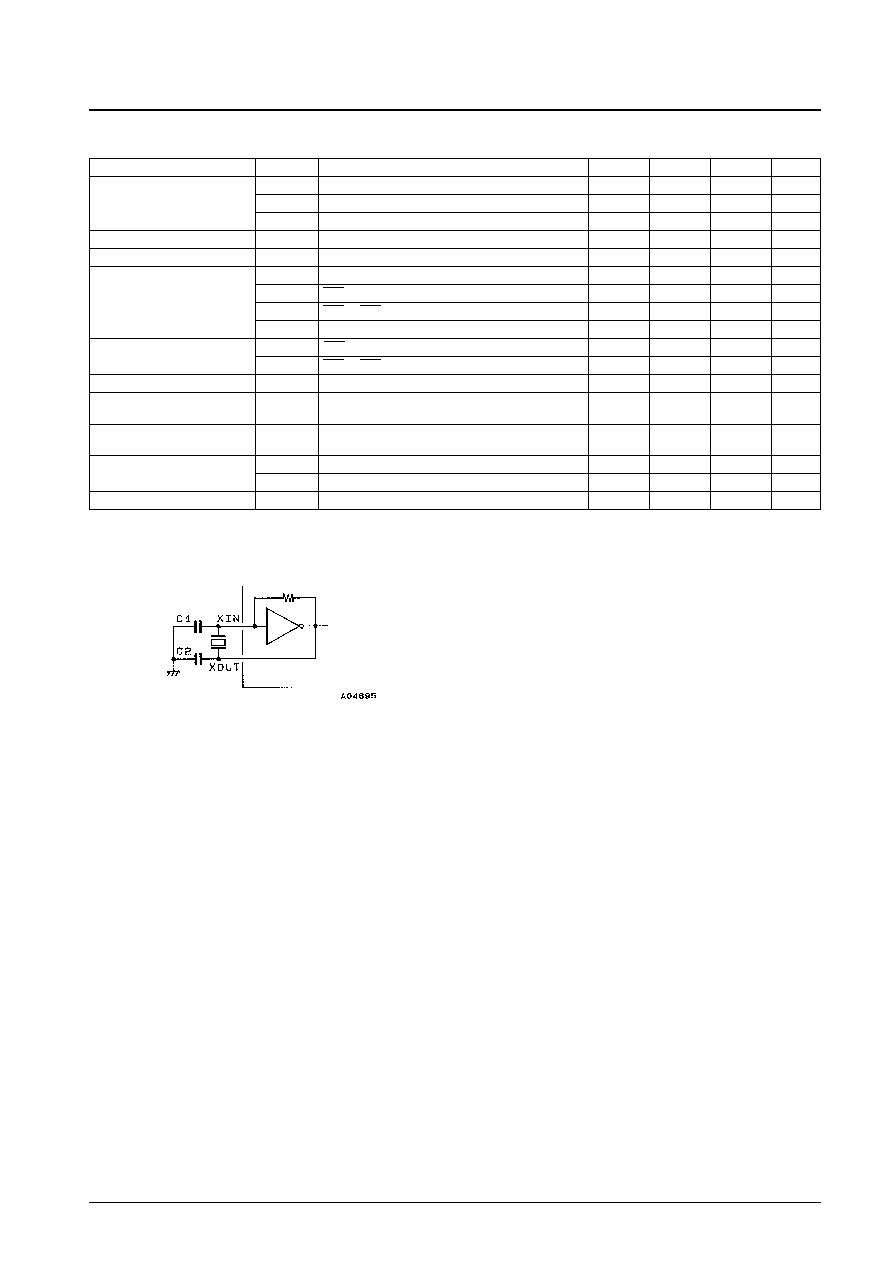
Oscillator Circuit Example
Kinseki, Ltd.
HC43/U: 2114-84521 (1): CL = 10 pF, C1 = 15 (10 to 22) pF, C2 = 15 pF
HC43/U: 2114-84521 (2): CL = 16 pF, C1 = 22 (15 to 33) pF, C2 = 33 pF
Nihon Denpa Kogyou, Ltd.
NR-18: LM-X-0701: CL = 10 pF, C1 = 15 pF, C2 = 15 pF
Since the circuit constants in the crystal oscillator circuit depend on the crystal element used and the printed circuit board
pattern, we recommend consulting with the manufacturer of the crystal element concerning this circuit.
No. 5262-3/8
LM7001J, 7001JM
Parameter
Symbol
Conditions
min
typ
max
Unit
R
f1
XIN
1.0
M
Built-in feedback resistance
R
f2
FMIN
500
k
R
f3
AMIN
500
k
Input high-level current
I
IH
CE, CL, DATA: V
IN
= 6.5 V
5.0
µA
Input low-level current
I
IL
CE, CL, DATA: V
IN
= 0 V
5.0
µA
V
OL
1
FMIN, AMIN: I
OUT
= 0.5 mA
3.5
V
V
OL
2
SYC: I
OUT
= 0.1 mA,
*
1
0.02
0.3
V
Output low-level voltage
V
OL
3
BO1 to BO3: I
OUT
= 2.0 mA
1.0
V
V
OL
4
P
D
1, P
D
2: I
OUT
= 0.1 mA
0.3
V
Output off leakage current
I
OFF
1
SYC: V
OUT
= 6.5 V
5.0
µA
I
OFF
2
BO1 to BO3: V
OUT
= 13 V
3.0
µA
Output high-level voltage
V
OH
P
D
1, P
D
2: I
OUT
= ≠0.1 mA
0.5 V
DD
V
High-level 3-state
I
OFFH
P
D
1, P
D
2: V
OUT
= V
DD
0.01
10.0
nA
off leakage current
Low-level 3-state
I
OFFL
P
D
1, P
D
2: V
OUT
= 0 V
0.01
10.0
nA
off leakage current
Current drain
I
DD
1
V
DD
1 + V
DD
2:
*
2
25
40
mA
I
DD
2
V
DD
2: PLL block stopped
2.0
3.5
mA
Input capacitance
C
IN
FMIN
1
2
3
pF
Equivalent Circuit Block Diagram
Pin Functions
No. 5262-4/8
LM7001J, 7001JM
Symbol
Description
SYC
Controller clock (400 kHz)
XIN, XOUT
Crystal oscillator (7.2 MHz)
FMIN, AMIN
Local oscillator signal input
CE, CL, DATA
Data input
BO1 to BO3
Band data output. BO1 can be used as a time base output (8 Hz).
V
DD
1, V
DD
2, V
SS
Power supply (Apply power to both V
DD
1 and V
DD
2 when the PLL circuit is operating. V
DD
2 is the crystal oscillator and time base
power supply. Internal data cannot be maintained on V
DD
2 only.)
P
D
1, P
D
2
Charge pump output
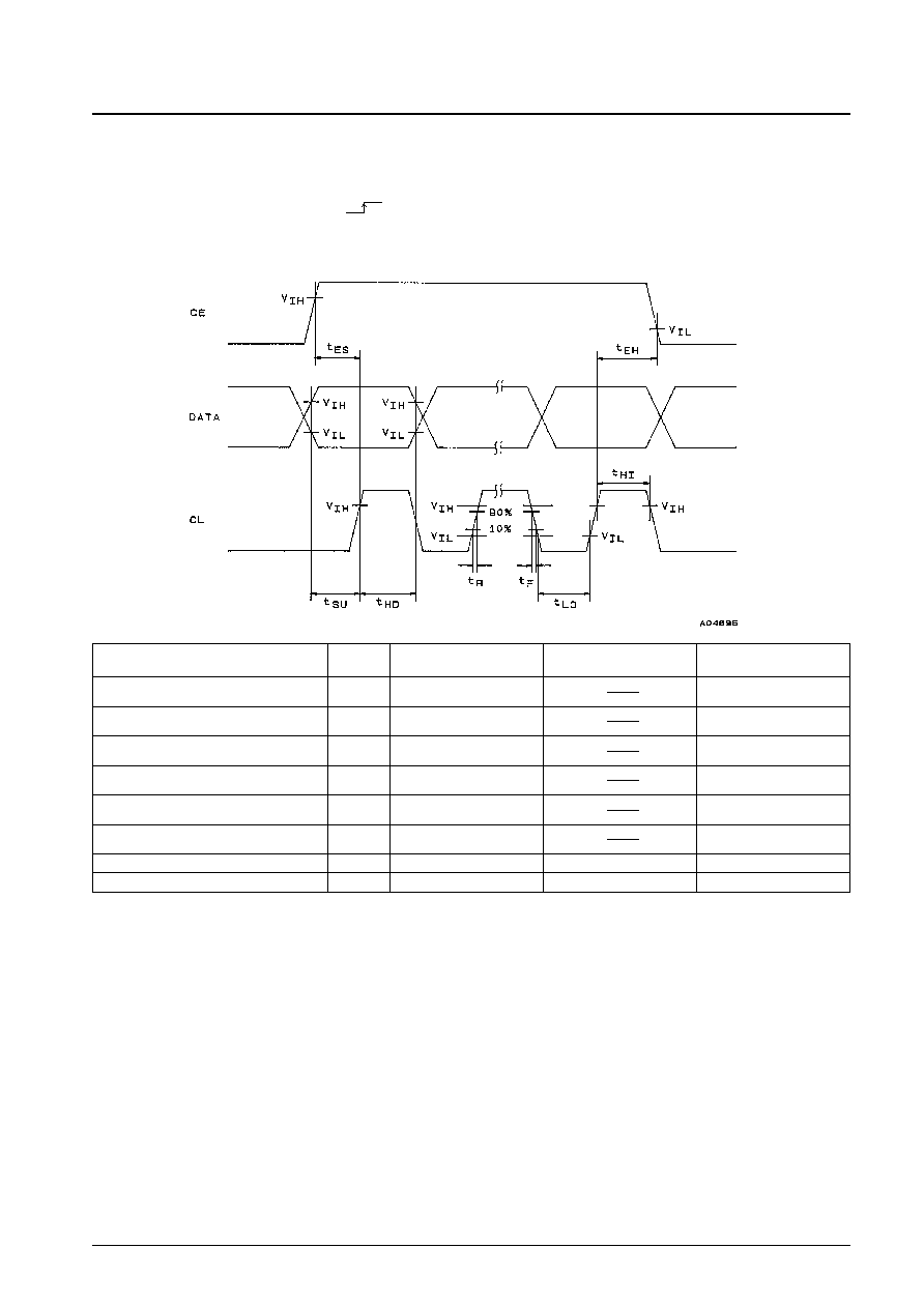
Data Input Timing
V
IH
= 2.2 to 6.5 V, V
IL
= 0 to 0.7 V, Xtal = 5.00 to 7.20 (typ) to 8.00 MHz
Data acquisition: On the CL rising edge
Note: Data transfers must be started only after the crystal oscillator is operating normally, i.e., after a proper input signal
has been supplied to XIN.
No. 5262-5/8
LM7001J, 7001JM
Parameter
Symbol
Xtal: 7.20 MHz
Xtal: for frequencies
Example: XIN = 2.048 MHz
other than 7.2 MHz
Enable setup time
t
ES
At least 1.5 µs
At least [
]
◊
1.35
At least 5.27 µs
Enable hold time
t
EH
At least 1.5 µs
At least [
]
◊
1.35
At least 5.27 µs
Data setup time
t
SU
At least 1.5 µs
At least [
]
◊
1.35
At least 5.27 µs
Data hold time
t
HD
At least 1.5 µs
At least [
]
◊
1.35
At least 5.27 µs
Clock low-level time
t
LO
At least 1.5 µs
At least [
]
◊
1.35
At least 5.27 µs
Clock high-level time
t
HI
At least 1.5 µs
At least [
]
◊
1.35
At least 5.27 µs
Rise time
t
R
Up to 1 µs
Up to 1 µs
Up to 1 µs
Fall time
t
F
Up to 1 µs
Up to 1 µs
Up to 1 µs
1
◊
8
f Xtal
1
◊
8
f Xtal
1
◊
8
f Xtal
1
◊
8
f Xtal
1
◊
8
f Xtal
1
◊
8
f Xtal
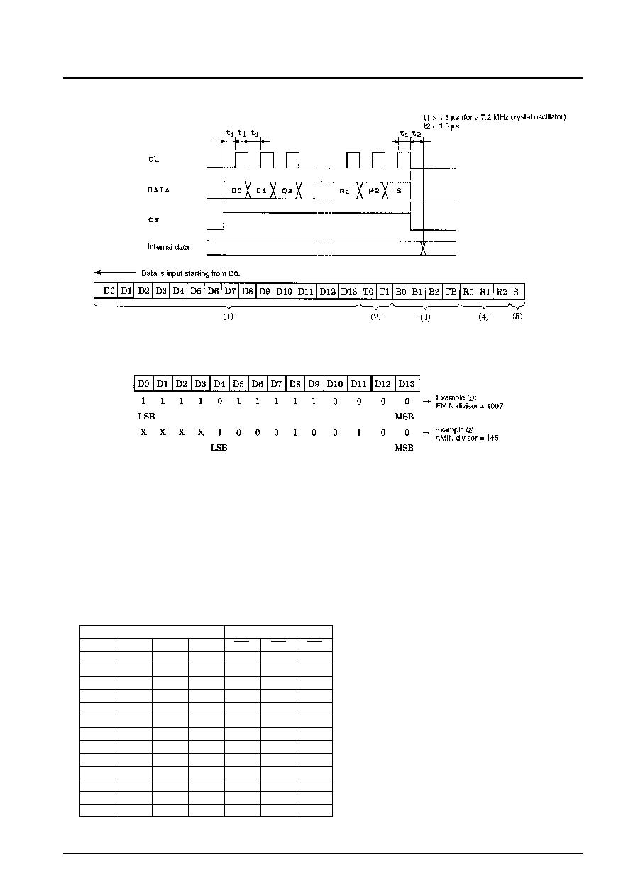
Data Input
(1) D0 (LSB) to D13 (MSB): Divisor data
FMIN uses D0 to D13 and AMIN uses D4 to D13.
Sample calculation
x FM 100 kHz steps (f
ref
= 100 kHz)
FM VCO = 100.7 MHz (FM RF = 90.0 MHz, IF = 10.7 MHz)
Divisor =
100.7 MHz (FM VCO) ˜ 100 kHz (f
ref
) = 1007
3EF
(HEX)
y AM 10 kHz steps (f
ref
= 10 kHz)
AM VCO = 1450 kHz (AM RF = 1000 kHz, IF = 450 kHz)
Divisor =
1450 kHz (AM VCO) ˜ 10 kHz (f
ref
) = 145
91
(HEX)
(2) T0 and T1 are LSI test bits and both should be set to 0.
(3) B0 to B2, TB: Band data
Time base data
Note:
*
: Determined by R0 to R3. See item (4) on next page.
!
: Don't care
TB: 8 Hz
No. 5262-6/8
LM7001J, 7001JM
Input
Output
B0
B1
B2
TB
BO1
BO2
BO3
0
0
0
0
*
*
*
0
0
1
0
0
0
1
0
1
0
0
0
1
0
0
1
1
0
0
1
1
1
0
0
0
1
0
0
1
0
1
0
1
0
1
1
1
0
0
1
1
0
1
1
1
0
1
1
1
0
0
0
1
TB
*
*
!
1
0
1
TB
1
0
!
0
1
1
TB
0
1
!
1
1
1
TB
1
1
1
0
0
1
TB
0
0
(4) R0 to R2: Reference frequency data
Note: The values listed for BO1, BO2, and BO3 are for the case when the B0 to B2 data is set to all zeros.
(5) S: Divider selection data
1: FMIN, 0: AMIN
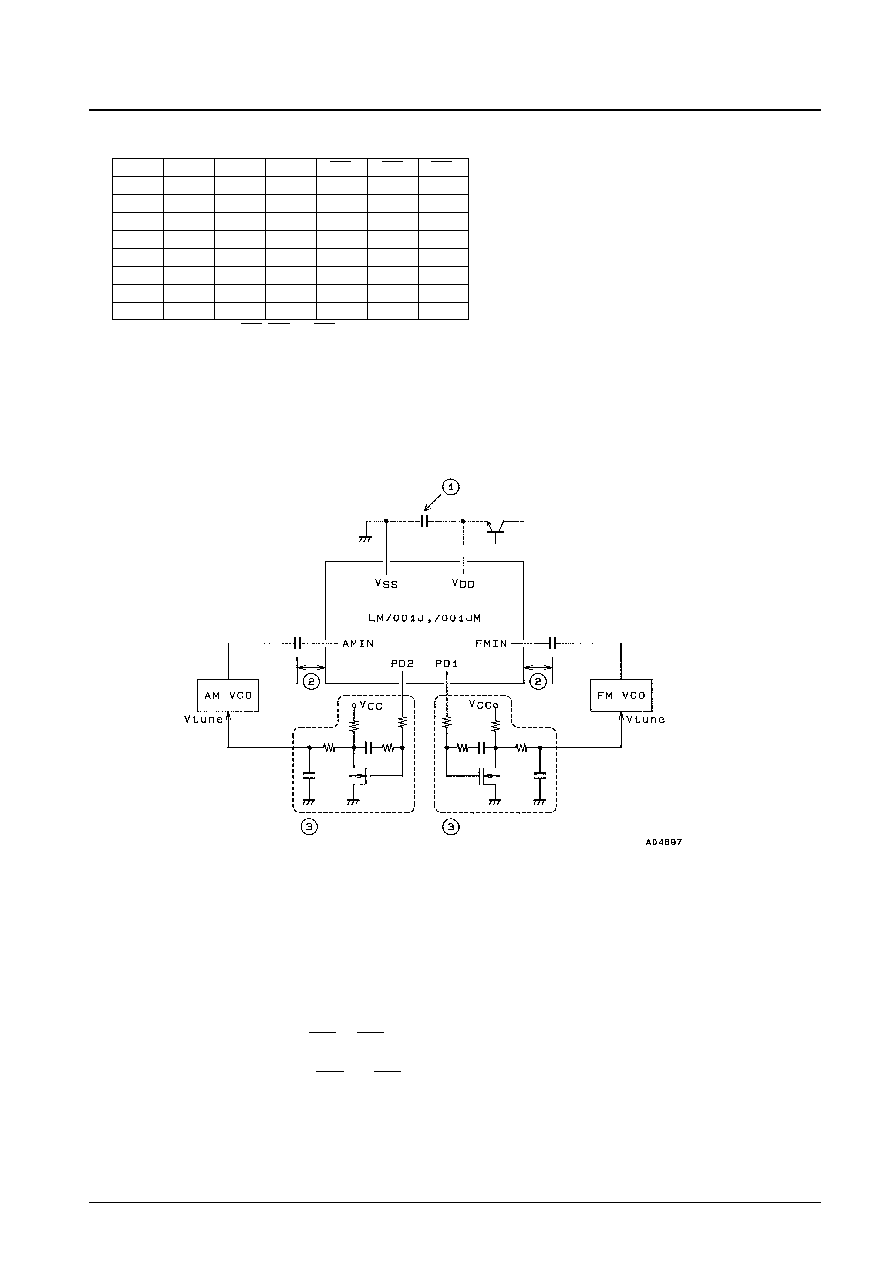
Notes on PLL IC Usage
1. PLL IC printed circuit board patterns
x Power supply pins
A capacitor must be inserted between the V
DD
and V
SS
power supply pins for noise exclusion. This capacitor
must be located as close as possible to these pins.
y FMIN and AMIN pins
The coupling capacitors must be located as close as possible to these pins.
z PD pins, low-pass filter
Since those are high-impedance pins, they are susceptible to noise. Therefore, the pattern should be kept as short
as possible and the area around this circuit should be covered by the ground pattern.
2. Initial states of the output ports (BO1 to BO3)
The initial states of the output ports after power is applied are undefined until data has been transferred.
In particular, it is possible for the BO1 and BO3 pins to output the internal clock, so data must be transferred as soon
as possible.
However, note that the LSI cannot accept data until the crystal oscillator is operating normally.
No. 5262-7/8
LM7001J, 7001JM
R0
R1
R2
f
ref [
kHz]
BO1
BO2
BO3
0
0
0
100
1
1
0
0
0
1
50
1
1
0
0
1
0
25
1
1
0
0
1
1
5
0
0
1
1
0
0
10
1
0
1
1
0
1
9
1
0
1
1
1
0
1
0
1
1
1
1
1
5
0
0
1

No. 5262-8/8
LM7001J, 7001JM
3. VCO
The VCO circuit is designed so that it does not stop oscillating even if the control voltage (Vtune) becomes 0 V.
(This is because the PLL circuit could become deadlocked if the VCO stopped.)
This catalog provides information as of February, 1997. Specifications and information herein are subject to
change without notice.
s
No products described or contained herein are intended for use in surgical implants, life-support systems, aerospace
equipment, nuclear power control systems, vehicles, disaster/crime-prevention equipment and the like, the failure of
which may directly or indirectly cause injury, death or property loss.
s
Anyone purchasing any products described or contained herein for an above-mentioned use shall:
Accept full responsibility and indemnify and defend SANYO ELECTRIC CO., LTD., its affiliates, subsidiaries and
distributors and all their officers and employees, jointly and severally, against any and all claims and litigation and all
damages, cost and expenses associated with such use:
Not impose any responsibility for any fault or negligence which may be cited in any such claim or litigation on
SANYO ELECTRIC CO., LTD., its affiliates, subsidiaries and distributors or any of their officers and employees
jointly or severally.
s
Information (including circuit diagrams and circuit parameters) herein is for example only; it is not guaranteed for
volume production. SANYO believes information herein is accurate and reliable, but no guarantees are made or implied
regarding its use or any infringements of intellectual property rights or other rights of third parties.