SPI-236-17
No.6025 1/6
Features
∑
GaAs Infrared LED plus Single Phototransistor
∑
Photo-Interrupter
∑
Contact type
∑
Compact type : H3.25 ! L5.0 ! W4.5mm
∑
Application : For the general public welfare
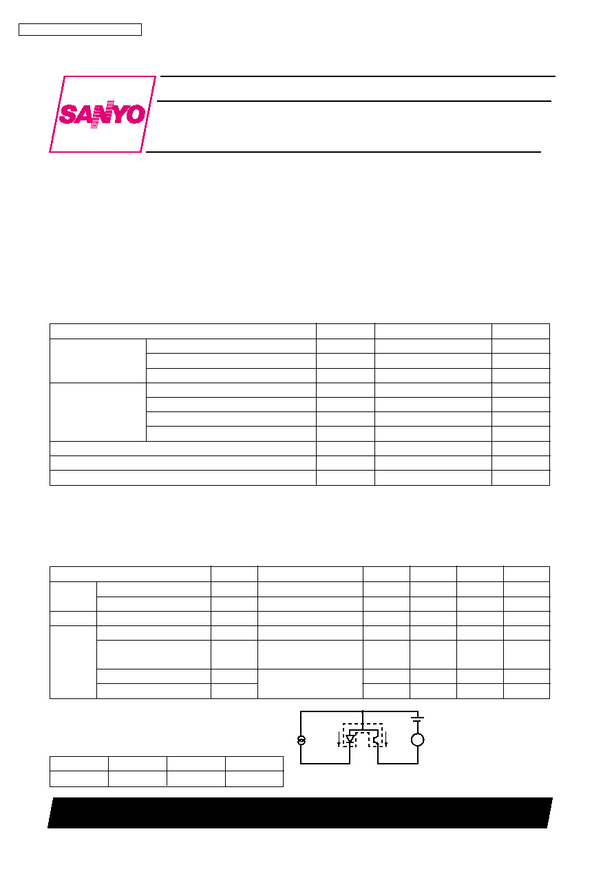
Absolute Maximum Ratings at Ta=25
∞
C, 65%RH (as per JIS C 7032 )
Parameter
Symbol
Rating
Unit
Input LED
Forward Current
*1
I
F
50
mA
Reverse Voltage
V
R
5
V
Power Dissipation
P
D
70
mW
Output
Collector-Emitter Voltage
V
CEO
20
V
Phototransistor
Emitter-Collector Voltage
V
ECO
5
V
Collector Curren
I
C
20
mA
Power Dissipation
P
C
70
mW
Operating Temperature
Topr
--20 to +80
∞
C
Storage Temperature
Tstg
--30 to +85
∞
C
Soldering Temperature
*2
Tsol
260
∞
C
*1
See forward current derating
*2
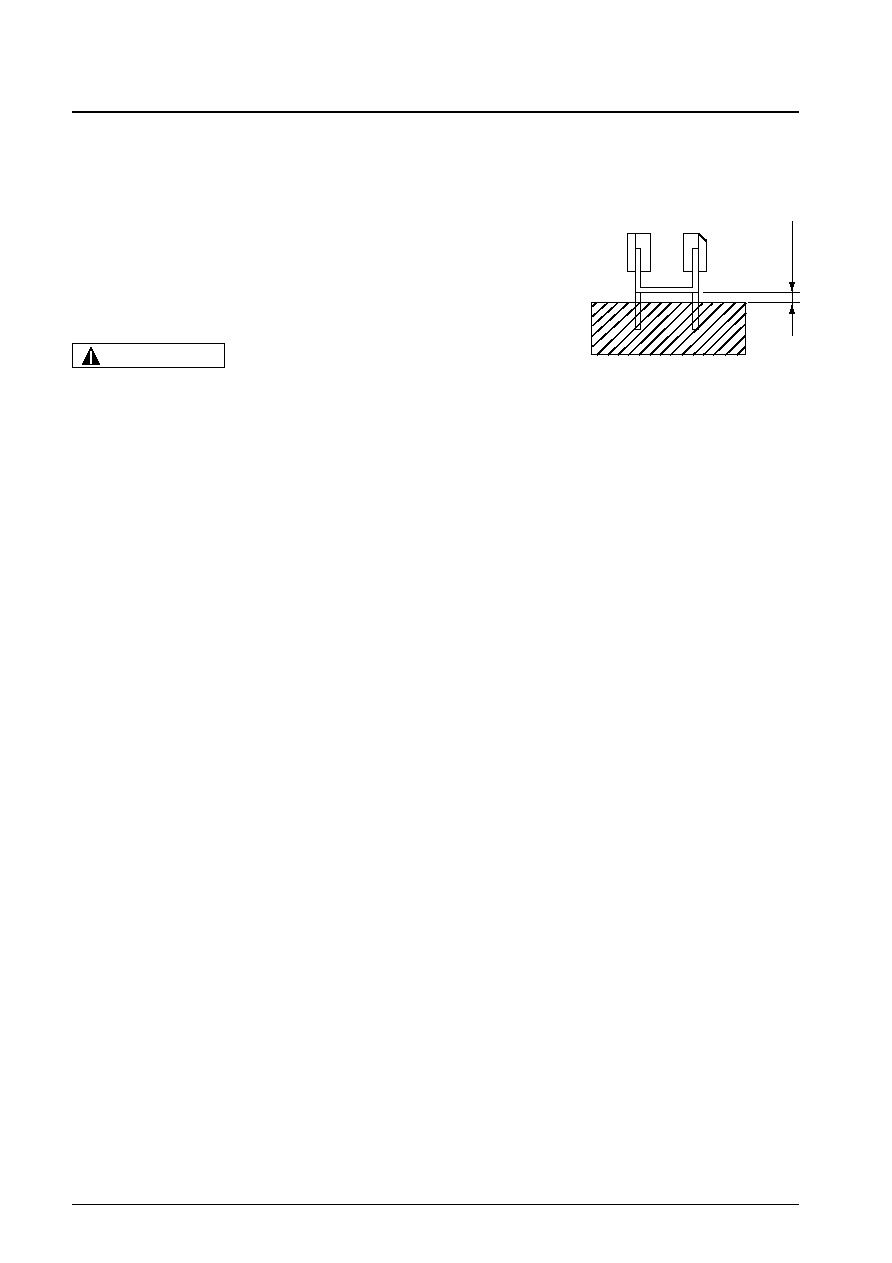
Soldering conditions : time : max. 3sec; clearance : min. 1mm from lower stay
Electro-Optical Characteristics at Ta=25
∞
C, 65%RH
Parameter
Symbol
Condition
Min.
Typ.
Max.
Unit
Input
Forward Voltage
V
F
I
F
=10mA
1.0
1.15
1.4
V
Reverse Current
I
R
V
R
=5V
--
--
10
µ
A
Output
Dark Current
I
CEO
I
F
=0mA, V
CE
=10V
--
10
200
nA
Coupled
Collector Output Current
I
C
I
F
=10mA, V
CE
=5V
*1
240
500
880
µ
A
Collector Emitter
V
CE
(sat)
I
F
=10mA, I
C
=50
µ
A
--
--
0.5
V
Saturation Voltage
Rise Time
tr
V
CC
=5V, R
L
=100
--
5
--
µ
s
Fall Time
tf
I
C
=1mA
--
5
--
µ
s
*1
Measurement Circuit of Collector Current
*2
Table of Classification of Collector Output
Class
A
B
C
Ic (
µ
A)
880 to 460
635 to 330
460 to 240
SANYO Electric Co.,Ltd. Semiconductor Company
TOKYO OFFICE Tokyo Bldg., 1-10, 1 Chome, Ueno, Taito-ku, TOKYO, 110-8534 JAPAN
SPI-236-17
GaAs Infrared LED
Ultraminiature photointerrupter
(single-transistor type)
72199 GI, (MI)
IF=10mA
VCE=5V
A
Ic
Ordering number : EN6025
SPI-236-17
No.6025 2/6
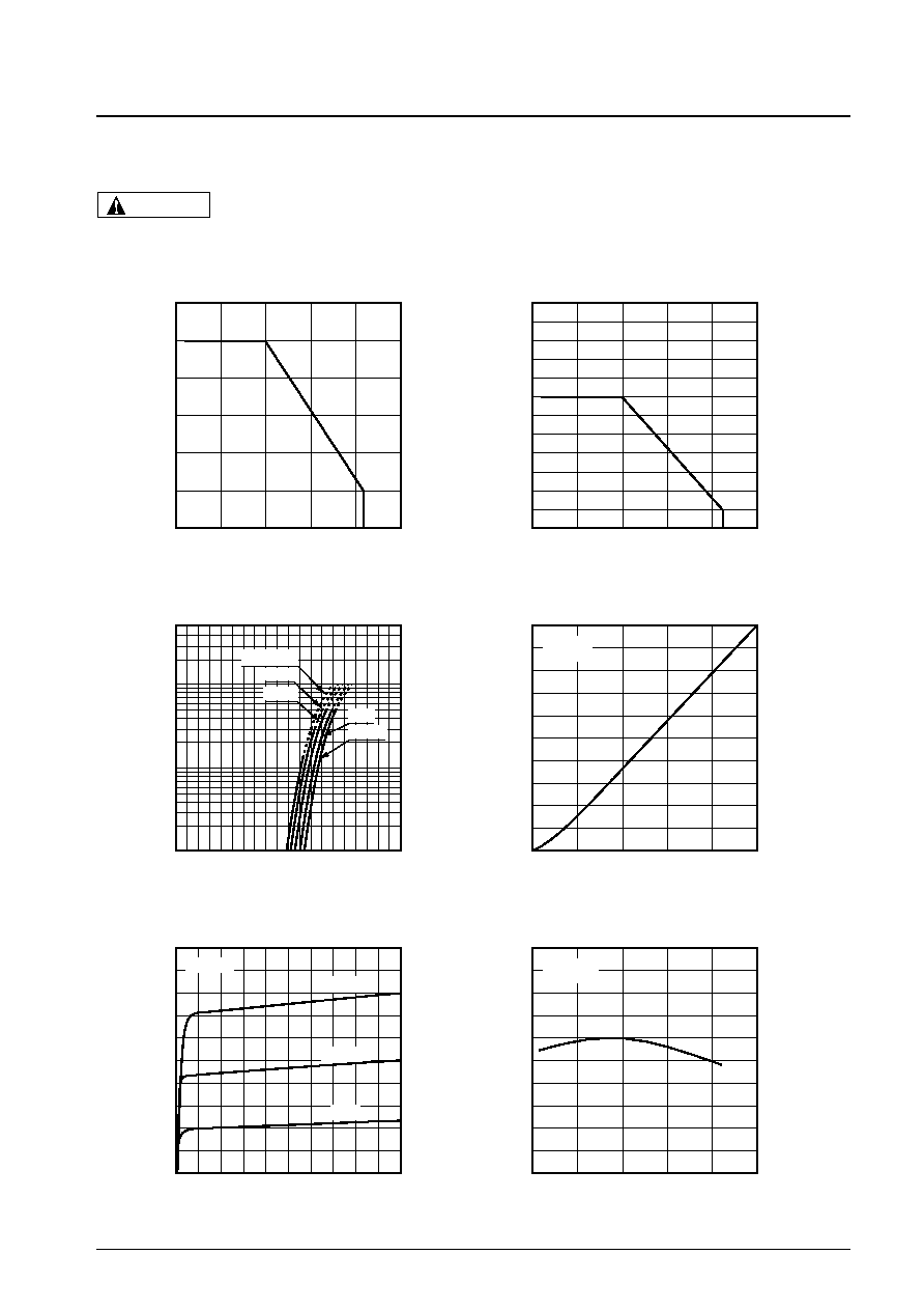
Typical Characteristics
These numerical value show the electrical and optical characteristics of this product, and not assure this contents.
CAUTION
60
50
40
30
20
10
0
--25
0
25
50
75
100
120
100
80
60
40
20
0
--25
0
25
50
75
100
500
100
50
10
5
1
0
0.5
1
1.5
2
0
200
400
600
800
1000
0
4
8
12
16
20
Ta=75
∞
C
50
∞
C
25
∞
C
0
∞
C
--25
∞
C
VCE=5V
Ta=25
∞
C
0
5
10
40
60
80
100
120
140
0
200
400
600
800
1000
--25
0
25
50
75
100
IF=10mA
VCE=5V
Ta=25
∞
C
IF=15mA
10mA
5mA
Forward Current vs. Ambient Temperature
Collector Current vs. Collector-emitter Voltage
Ambient Temperature Ta (
∞
C)
Collector-emitter Voltage VCE (V)
F
orw
ard Current I
F
(mA)
Collector Current I
C
(
µ
A)
Forward Current vs. Forward Voltage
Forward Voltage VF (V)
F
orw
ard Current I
F
(mA)
(Rating)
Power Dissipation vs. Ambient Temperature
Relative Collector Current vs. Ambient Temperature
Ambient Temperature Ta (
∞
C)
Ambient Temperature Ta (
∞
C)
Po
wer Dissipation P (mW)
Relati
v
e
Collector Current (%)
Collector vs. Forward Current
Forward Current IF (mA)
Collector Current I
C
(
µ
A)
(Rating)
SPI-236-17
No.6025 3/6
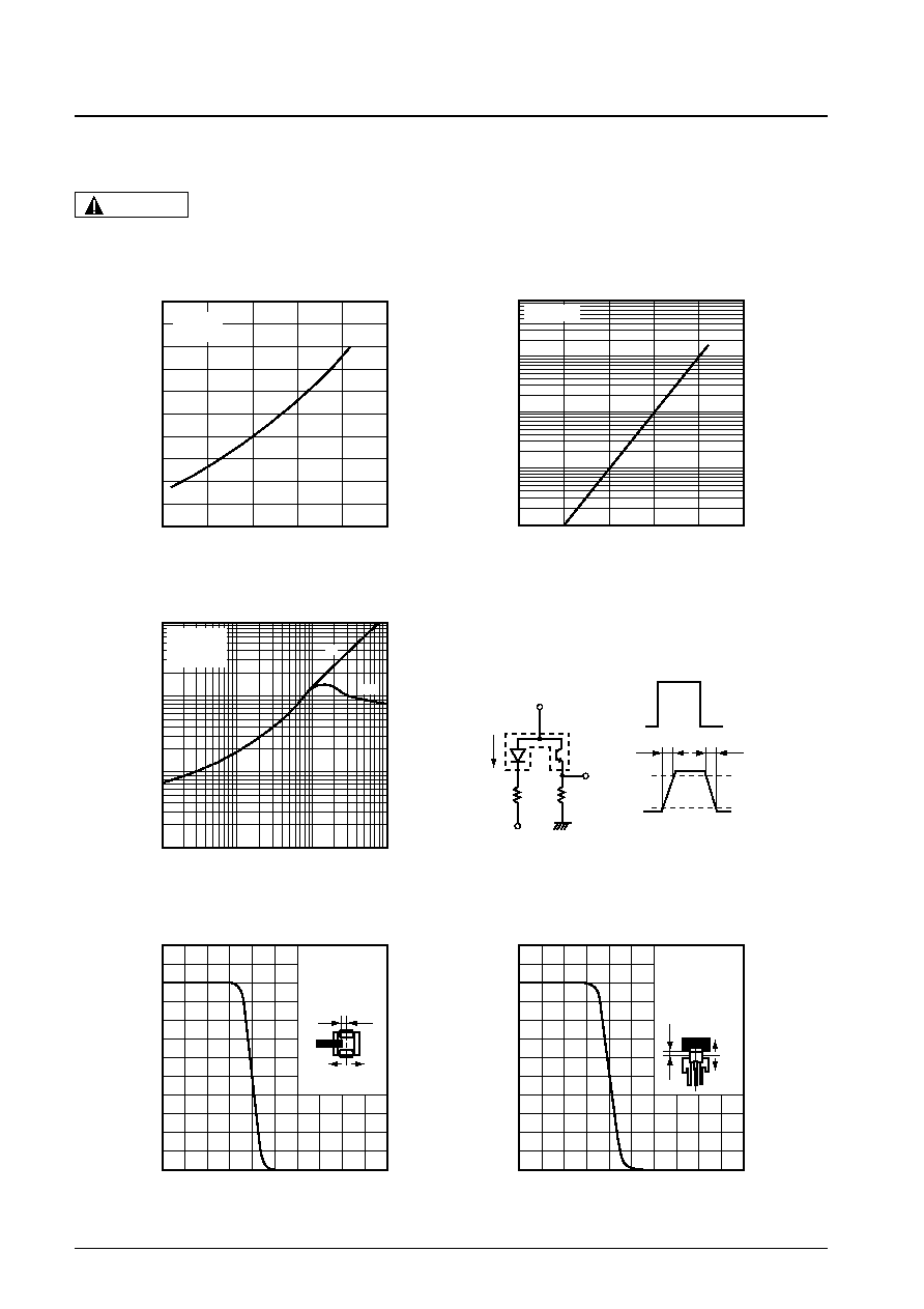
Typical Characteristics
These numerical value show the electrical and optical characteristics of this product, and not assure this contents.
CAUTION
10
-6
5
10
-7
5
10
-8
5
10
-9
10
-10
5
--25
0
25
50
75
100
120
100
80
60
40
20
0
--2
--1
0
1
2
3
1000
500
100
50
10
5
1
0.1
0.5 1
5
10
50
100
0.08
0.10
0.12
0.14
0.16
0.18
--25
0
25
50
75
100
IF=10mA
IC=50
µ
A
VCE=10V
IFP=10mA
VCC=5V
Ta=25
∞
C
IF=10mA
VCE=5V
Ta=25
∞
C
d
tf
tr
0
+
120
100
80
60
40
20
0
--2
--1
0
1
2
3
IF=10mA
VCE=5V
Ta=25
∞
C
IFP
VCC
RL
Vout
Vout
IFP
RD
d
0
+
10%
90%
tr
tf
--
Shield
Shield
Detector center
Detector center
--
Collector-emitter Saturation Voltage vs.
Ambient Temperature
Relative Collector Current vs. Shield Distance (1)
Relative Collector Current vs. Shield Distance (2)
Ambient Temperature Ta (
∞
C)
Shield Distance d (mm)
Collector
-emitter
Saturation V
oltage V
CE (sat)
(V)
Relati
v
e
Collector Current (%)
Shield Distance d (mm)
Relati
v
e
Collector Current (%)
Response Time vs. Load Resistance
Test Circuit for Response Time
Load Resistance RL (k
)
Response (
µ
S
)
Collector Dark Current vs. Ambient Temperature
Ambient Temperature Ta (
∞
C)
Collector Dark Current I
CEO
(A)
SPI-236-17
No.6025 4/6
Ph.Tr
LED
Pin connection
1. Common (Anode)
2. LED Cathode
3. Ph. Tr Emitter
Pin No.
0.5, Max 0.1
3
1
2
2.4
2.5
3
4.5
0.25
3.5
0.25
0.25
1.5
5
±
0.3
2
±
0.3
1.5
2.9
1.3
0.3, Max 0.1
3.25
2.4
2.7
2.8
1.5
1
1
Optical C / L
Injection gate
C0.5
3--0.4
2
Tolerance :
±
0.2
Unit
: mm
SPI-236-17
No.6025 5/6
Package dimensions and Pin connection
As stated in the sttached paper. (No.6025 4/6)
Soldering conditions
(1) Temperature
: Max. 260
∞
C
(2) Time
: Max. 3 sec
(3) Clearance
: Min. 1mm from stay (include PCB thickness)
(1) Bending a lead should avoid. However, when bending is necessary, take care the next items.
q Bending a lead must be done before soldering.
w Bending a lead must be done in the states of fixing leads and no stress for the regin part. Because it is possible that
stress for the regin part cause troubles such as gold wire breaking and so on.
e A lead must be bend under the stay.
r Do not bend the same position of leads more than twice.
(2) The hole pitch of a circuit board must fit to the lead pitch.
(3) Two stays coupling LED and Ph. Tr should be isolated from any PCB pattern or any lead.
(4) Take core the following when soldering.
q Do not heat a product under any stress (a twist and so on) to leads.
w Do not heat a product in the states of operating force to the regin part.
(5) Use the flux which contain no chlorine, have no corrosion and do not need washing.
(6) Be careful that flux or other chemicals do not attach to the luminous surface and passive surface.
PRECAUTIONS
Min.
1mm