SPI-240-15-T1
No.6027 1/7
Features
∑
GaAs Infrared LED plus Darlington Phototransistor
∑
Photo-Interrupter for reflow soldering
∑
Compact type : H4.95 ! L6.0 ! W5.5mm
∑
Taping type
Absolute Maximum Ratings at Ta=25
∞
C, 65%RH
Parameter
Symbol
Rating
Unit
Input LED
Forward Current
I
F
50
mA
Reverse Voltage
V
R
5
V
Power Dissipation
P
D
70
mW
Output
Collector-Emitter Voltage
V
CEO
20
V
Phototransistor
Emitter-Collector Voltage
V
ECO
5
V
Collector Curren
I
C
20
mA
Power Dissipation
P
C
70
mW
Operating Temperature
Topr
--20 to +80
∞
C
Storage Temperature
Tstg
--30 to +85
∞
C
Electro-Optical Characteristics at Ta=25
∞
C, 65%RH
Parameter
Symbol
Condition
Min.
Typ.
Max.
Unit
Input
Forward Voltage
V
F
I
F
=10mA
1.0
1.15
1.4
V
Reverse Current
I
R
V
R
=5V
--
--
10
µ
A
Output
Dark Current
I
CEO
I
F
=0mA, V
CE
=10V
--
--
1
µ
A
Coupled
Collector Output Current
I
C
I
F
=4mA, V
CE
=2V
*1
0.5
3
--
mA
Collector Emitter
V
CE
(sat)
I
F
=4mA, I
C
=250
µ
A
--
--
1.2
V
Saturation Voltage
Rise Time
tr
V
CC
=5V, R
L
=100
--
100
--
µ
s
Fall Time
tf
I
C
=10mA
--
100
--
µ
s
*1
Measurement Circuit of Collector Current
SANYO Electric Co.,Ltd. Semiconductor Company
TOKYO OFFICE Tokyo Bldg., 1-10, 1 Chome, Ueno, Taito-ku, TOKYO, 110-8534 JAPAN
SPI-240-15-T1
GaAs Infrared LED
Ultraminiature photointerrupter supporting reflow soldering
(Darlington-transistor type)
72199 GI, (MI)
IF=4mA
VCE=2V
A
Ic
Ordering number : EN6027
SPI-240-15-T1
No.6027 2/7
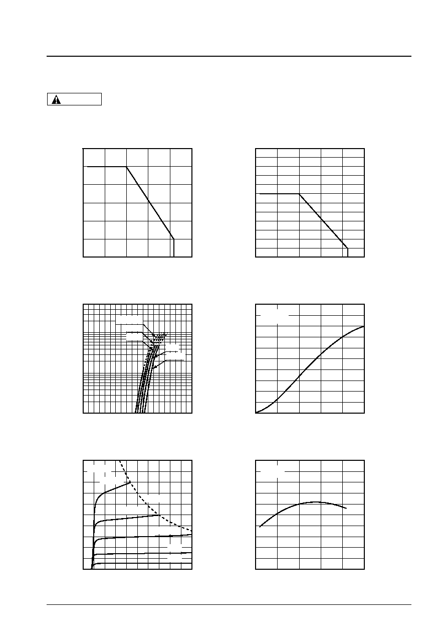
Typical Characteristics
These numerical value show the electrical and optical characteristics of this product, and not assure this contents.
CAUTION
60
50
40
30
20
10
0
-25
0
25
50
75
100
120
100
80
60
40
20
0
-25
0
25
50
75
100
500
100
50
10
5
1
0
0.5
1
1.5
2
0
2
4
6
8
10
12
14
16
18
20
0
4
8
12
16
20
Ta=75
∞
C
50
∞
C
25
∞
C
0
∞
C
--25
∞
C
VCE=2V
Ta=25
∞
C
0
5
10
40
60
80
100
120
140
0
2
4
6
8
10
12
14
16
18
20
--25
0
25
50
75
100
IF=4mA
VCE=2V
Ta=25
∞
C
Pc(MAX)
IF=15mA
10mA
4mA
7mA
2mA
Forward Current vs. Ambient Temperature
Collector Current vs. Collector-emitter Voltage
Ambient Temperature Ta (
∞
C)
Collector-emitter Voltage VCE (V)
F
orw
ard Current I
F
(mA)
Collector Current I
C
(
µ
A)
Forward Current vs. Forward Voltage
Forward Voltage VF (V)
F
orw
ard Current I
F
(mA)
Power Dissipation vs. Ambient Temperature
Relative Collector Current vs. Ambient Temperature
Ambient Temperature Ta (
∞
C)
Ambient Temperature Ta (
∞
C)
Po
wer Dissipation P (mW)
Relati
v
e
Collector Current (%)
Collector vs. Forward Current
Forward Current IF (mA)
Collector Current I
C
(mA)
(Rating)
(Rating)
SPI-240-15-T1
No.6027 3/7
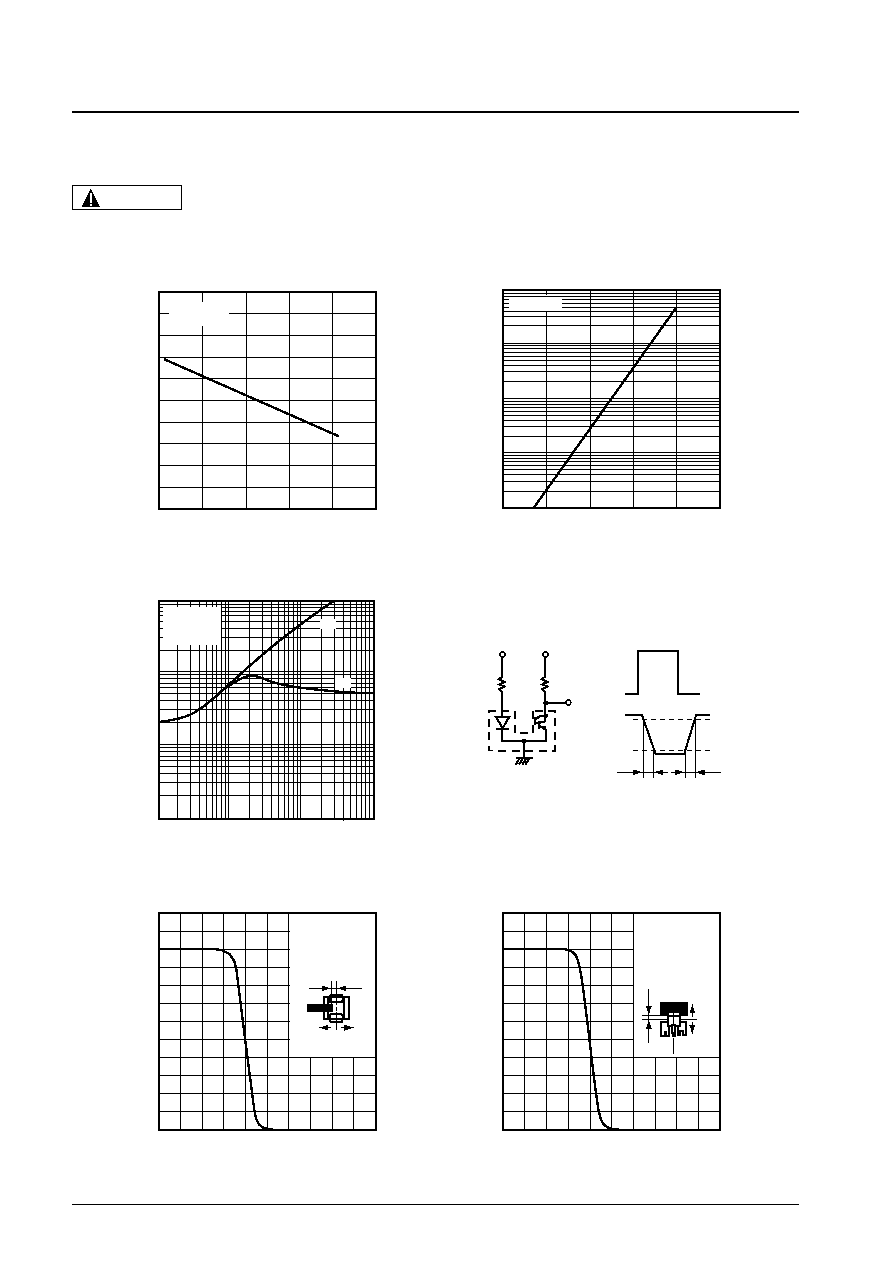
Typical Characteristics
These numerical value show the electrical and optical characteristics of this product, and not assure this contents.
CAUTION
10
-5
5
10
-6
5
10
-7
5
10
-8
10
-9
5
--25
0
25
50
75
100
120
100
80
60
40
20
0
--2
--1
0
1
2
3
1000
500
100
50
10
5
1
10
50
100
500
1k
5k
10k
0.5
0.6
0.7
0.8
0.9
1.0
--25
0
25
50
75
100
IF=4mA
IC=250
µ
A
VCE=10V
IFP=10mA
VCC=2V
Ta=25
∞
C
IF=4mA
VCE=2V
Ta=25
∞
C
d
t f
t r
0
+
120
100
80
60
40
20
0
--2
--1
0
1
2
3
IF=4mA
VCE=2V
Ta=25
∞
C
IFP
VCC
RL
Vout
Vout
IFP
RD
d
0
+
10%
90%
tr
tf
Collector-emitter Saturation Voltage vs.
Ambient Temperature
Relative Collector Current vs. Shield Distance (1)
Relative Collector Current vs. Shield Distance (2)
Ambient Temperature Ta (
∞
C)
Shield Distance d (mm)
Collector
-emitter
Saturation V
oltage V
CE (sat)
(V)
Relative Collector Current (%)
Shield Distance d (mm)
Relative Collector Current (%)
Response Time vs. Load Resistance
Test Circuit for Response Time
Load Resistance RL (
)
Response (
µ
S
)
Collector Dark Current vs. Ambient Temperature
Ambient Temperature Ta (
∞
C)
Collector Dark Current I
CEO
(A)
--
Shield
Shield
Detector center
Detector center
--

SPI-240-15-T1
No.6027 4/7
Pin No.
3
1
2
2.5
3-0.4
3.5
5.5
Ph.Tr
LED
2
4.5
2
0.25
1.5
1.5
4.95
4.1
2.7
2.8
3.2
1
1
Optical C / L
Injection gate
C0.5
2.5
0.25
0.25
+ 0.1
-
-
0.2
0.6, Max 0.1
Pin connection
1. Ph. Tr Collector
2. Common (Cathode)
3. LED Anode
6
±
0.3
3
±
0.3
Tolerance :
±
0.2
Unit
: mm
SPI-240-15-T1
No.6027 5/7
Package dimensions and Pin connection
As stated in the sttached paper. (No.6027 4/7)
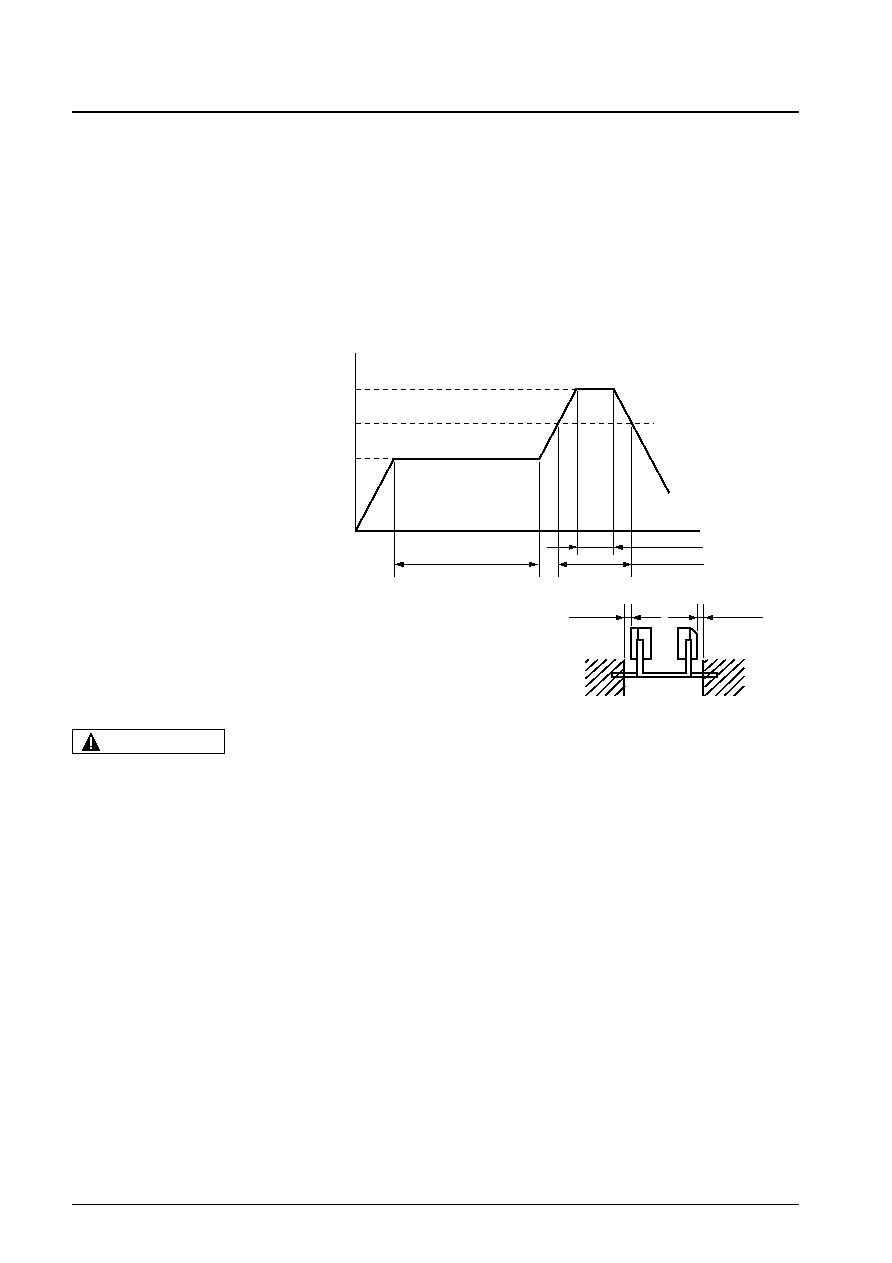
Soldering conditions
(1) Reflow soldering
The temperature of the reflow furnace is to be set in accordance with the following temperature profile.
Soldering must be done only one time.
Temperature
: On the topsurface of product
Reflow type
: Hot air
(2) Manusl soldering
Temperature
: Max. 290
∞
C (Soldering iron tip temperature)
Time
: Max. 3 sec
Clearance
: Min. 0.5mm from package
(1) Bending a lead should avoid. However, when bending is necessary, take care the next items.
q Bending a lead must be done before soldering.
w Bending a lead must be done in the states of fixing leads and no stress for the regin part. Because it is possible that
stress for the regin part cause troubles such as gold wire breaking and so on.
e A lead must be bend under the stay.
r Do not bend the same position of leads more than twice.
(2) The hole pitch of a circuit board must fit to the recommended mounting dimension.
(3) Take core the following when soldering.
q Do not heat a product under any stress (a twist and so on) to leads.
w Do not heat a product in the states of operating force to the regin part.
(4) Use the flux which contain no chlorine, have no corrosion and do not need washing.
(5) Be careful that flux or other chemicals do not attach to the luminous surface and passive surface.
(6) Precautions of the product after the open dry packing
q The product after the open dry packing should be stored in the dry packing again.
The product should be kept under the conditions below, if the product is not stored in the dry paking.
Temperature
: 5 to 30
∞
C
Humidity
: Max 70%RH
Term
: Max 7days
w The product to be out the term without dry packing must be practiced baking.
Baking conditions
: +60
±
5
∞
C, 10 to 20Hr
(7) The reflow conditions must be confirmed that no problem by your reflow furnace.
PRECAUTIONS
Max 220
∞
C
180
∞
C
Max 160
∞
C
Max 60sec
0.5mm
0.5mm
Max 5sec
Max 40sec