SPI-335-34
No.6029 1/6
Features
∑
Infrared LED plus Phototransistor (single)
∑
DIP type
∑
Compact type : 3.4 (L) ! 2.7 (W) ! 1.5 (H) mm
∑
Visible light cut type
∑
Lead length : (L=3.5mm)
Absolute Maximum Ratings at Ta=25
∞
C, 65%RH
Parameter
Symbol
Rating
Unit
Input LED
Forward Current
I
F
50
mA
Reverse Voltage
V
R
5
V
Power Dissipation
P
D
70
mW
Output
Collector-Emitter Voltage
V
CEO
20
V
Phototransistor
Emitter-Collector Voltage
V
ECO
5
V
Collector Curren
I
C
20
mA
Power Dissipation
P
C
70
mW
Operating Temperature
Topr
--20 to +80
∞
C
Storage Temperature
Tstg
--40 to +100
∞
C
Soldering Temperature
*1
Tsol
260
∞
C
*1
Soldering conditions : time : max. 3sec; clearance : min. 1mm from lower case edge.
Electro-Optical Characteristics at Ta=25
∞
C, 65%RH
Parameter
Symbol
Condition
Min.
Typ.
Max.
Unit
Input
Forward Voltage
V
F
I
F
=10mA
1.0
1.2
1.6
V
Reverse Current
I
R
V
R
=5V
--
--
10
µ
A
Output
Dark Current
I
CEO
I
F
=0mA, V
CE
=10V
--
10
200
nA
Coupled
Collector Output Current
I
C
I
F
=4mA, V
CE
=5V
*1
33
--
180
µ
A
Leakage Current
I
LEAK
I
F
=10mA, V
CE
=5V
*2
--
--
1
µ
A
Collector Emitter
V
CE
(sat)
I
F
=10mA, I
C
=50
µ
A
--
--
0.5
V
Saturation Voltage
Rise Time
tr
V
CC
=5V, R
L
=100
--
5
--
µ
s
Fall Time
tf
I
C
=1mA
--
5
--
µ
s
*1
Location of reflector is show in Fig. 1.
*2
No reflector
*3
Table of Classification of Collector Output
Class
E
F
G
H
Ic (
µ
A)
180 to 110
140 to 80
100 to 50
65 to 33
Marking color
Orange
Green
White
Silver
SANYO Electric Co.,Ltd. Semiconductor Company
TOKYO OFFICE Tokyo Bldg., 1-10, 1 Chome, Ueno, Taito-ku, TOKYO, 110-8534 JAPAN
SPI-335-34
Infrared LED
Ultraminiature photoreflector
(single-transistor type)
72199 GI, (MI)
AL V.E. film
Glass plate (t : 1mm)
Fig. 1 Location of Reflector
Ordering number : EN6029
SPI-335-34
No.6029 2/6
Package dimensions and Pin connection
As stated in the sttached paper. (No.6029 5/6)
Rank marking of collector output
The bottom of the package is colored following the table of classification of collector output.
Lot marking
Color division shall be done as shown in the drawing. (Fig. 2)
Year of even number
: Front side
Year of odd number
: Back side
Color
Black
Blue
Red
Green
Orange
Brown
Part `A'
January
February
March
April
May
June
Part `B'
July
August
September
October
November
December
Soldering conditions
(1) Temperature
: Max. 260
∞
C
(2) Time
: Max. 3sec
(3) Clearance
: Min. 1mm from the case edge. (Fig. 3)
(1) Bending a lead should avoid. However, when bending is necessary, take care the next items.
q Bending a lead must be done before soldering.
w Bending a lead must be done in the states of fixing leads and no stress for the regin part. Because it is possible that
stress for the regin part cause troubles such as gold wire breaking and so on.
e A lead must be bend at intervals of 2mm from the case edge.
r Do not bend the same position of leads more than twice.
(2) The hole pitch of a circuit board must fit to the lead pitch.
(3) Take core the following when soldering.
q Do not heat a product under any stress (a twist and so on) to leads.
w Do not heat a product in the states of operating force to the regin part.
(4) Use the flux which contain no chlorine, have no corrosion and do not need washing.
(5) Be careful that flux or other chemicals do not attach to the luminous surface and passive surface.
PRECAUTIONS
A
Front side
B
Fig. 2
1mm
Fig. 3
SPI-335-34
No.6029 3/6
1.5
1
4
Pin No.
C 0.6
0.4
1.6
3
2
3.4
0.5
3.5
±
0.5
0.5
0.6
3.3
2.0
±
10
∞
±
10
∞
4 -- 0.4
4.0
2.7
2.6
M
g
M : Color marking of Ic class
0 to 20
∞
0 to 20
∞
4 -- 0.2
4
3
2
1
Pin Connection
1. Ph. Tr Emitter
2. Ph. Tr Collector
3. LED Cathode
4. LED Anode
Tolerance :
±
0.2
Unit :
mm
SPI-335-34
No.6029 4/6
Typical Characteristics
These numerical value show the electrical and optical characteristics of this product, and not assure this contents.
CAUTION
60
50
40
30
20
10
0
--25
0
25
50
75
100
120
100
80
60
40
20
0
--25
0
25
50
75
100
0
100
200
300
400
500
0
4
8
12
16
20
VCE=5V
Ta=25
∞
C
0
5
10
40
60
80
100
120
140
0
200
400
600
800
1000
--25
0
25
50
75
100
IF=10mA
VCE=5V
Ta=25
∞
C
IF=20mA
15mA
10mA
5mA
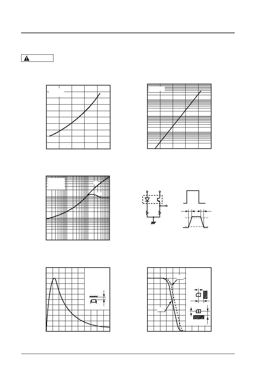
Forward Current vs. Ambient Temperature
Collector Current vs. Collector-emitter Voltage
Ambient Temperature Ta (
∞
C)
Collector-emitter Voltage VCE (V)
F
orw
ard Current I
F
(mA)
Collector Current I
C
(
µ
A)
(Rating)
Power Dissipation vs. Ambient Temperature
Relative Collector Current vs. Ambient Temperature
Ambient Temperature Ta (
∞
C)
Ambient Temperature Ta (
∞
C)
Po
wer Dissipation P (mW)
Relati
v
e
Collector Current (%)
Collector vs. Forward Current
Forward Current IF (mA)
Collector Current I
C
(
µ
A)
(Rating)
Ta=75
∞
C
50
∞
C
25
∞
C
0
∞
C
--25
∞
C
500
100
50
10
5
1
0
0.5
1
1.5
2
Forward Current vs. Forward Voltage
Forward Voltage VF (V)
F
orw
ard Current I
F
(mA)
SPI-335-34
No.6029 5/6
Typical Characteristics
These numerical value show the electrical and optical characteristics of this product, and not assure this contents.
CAUTION
10
-6
5
10
-7
5
10
-8
5
10
-9
10
-10
5
--25
0
25
50
75
100
120
100
80
60
40
20
0
0
1
2
3
4
5
1000
500
100
50
10
5
1
0.1
0.5
1
5
10
50
100
0.14
0.16
0.18
0.20
0.22
0.24
--25
0
25
50
75
100
IF=10mA
IC=50
µ
A
VCE=10V
IFP=20mA
VCC=5V
Ta=25
∞
C
IF=10mA
VCE=5V
Ta=25
∞
C
d
tf
tr
120
100
80
60
40
20
0
--4
--2
0
2
4
6
0
0
≠
≠
+
IFP
VCC
RL
Vout
Vout
IFP
RD
10%
90%
tr
tf
r1
r
2
r2
r1
+
Collector-emitter Saturation Voltage vs.
Ambient Temperature
Ambient Temperature Ta (
∞
C)
Collector
-emitter
Saturation V
oltage V
CE (sat)
(V)
Response Time vs. Load Resistance
Test Circuit for Response Time
Load Resistance RL (k
)
Response (
µ
S
)
Collector Dark Current vs. Ambient Temperature
Ambient Temperature Ta (
∞
C)
Collector Dark Current I
CEO
(A)
IF=10mA,VCE=5V
Ta=25
∞
C,d=1mm
Relative Collector Current vs. Distance
Relative Collector Current vs.
PPC paper Moving Distance
PPC paper Moving Distance r (mm)
Relati
v
e
Collector Current (%)
Distance between sensor and Ar evaporation d (mm)
Relati
v
e
Collector Current (%)