Overview
The STK311-010 is a hybrid integrated circuit (HIC) for
Radio Data System (RDS) applications which must
conform to European Broadcasting Union (EBU) enforced
recommendations. Since the Radio Data System (RDS)
subjects every kind of data to multiplex broadcasting for
FM broadcasts, the STK311-010 functions as a hybrid IC
which demodulates the modulated signal's data,
previously multiplexed to a RDS signal, matches
synchronization and performs error detection and
correction. By combining SC system and photoresist
technology with folded board construction and
incorporating Sanyo's unique insulated metal substrate
technology (IMST) to the base, the STK311-010 has
successfully been contained within a low-profile package.
Applications
∑ Car stereos
∑ Home stereos
Features
∑ On-chip 57 kHz BPF provides adjustment-free
performance
∑ On-chip 4 MHz ceramic oscillator
∑ Supports RDS data demodulation system designs
incorporating fewer external components
∑ On-chip ARI-SK/DK decoder
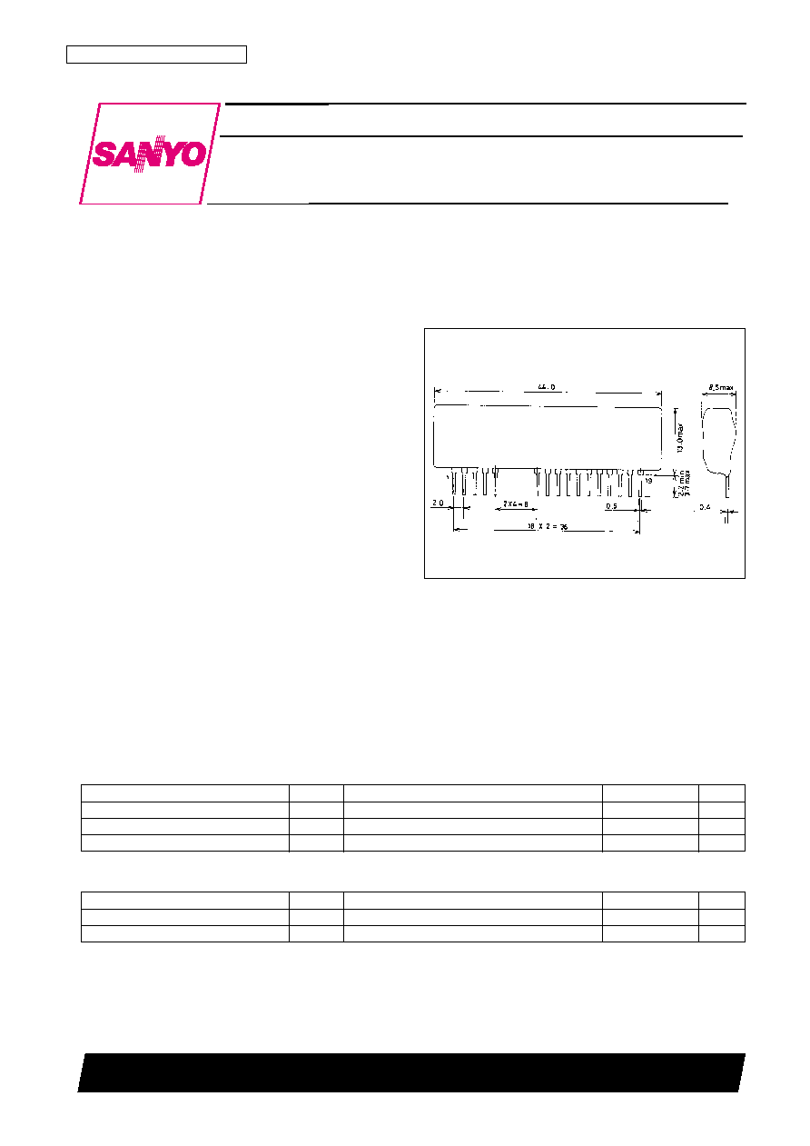
Package Dimensions
unit: mm
4132
Thick-Film Hybrid IC
N3096HA(OT)/10293YO 5-3279No. 4374-1/7
[STK311-010]
SANYO Electric Co.,Ltd. Semiconductor Bussiness Headquarters
TOKYO OFFICE Tokyo Bldg., 1-10, 1 Chome, Ueno, Taito-ku, TOKYO, 110 JAPAN
RDS Demodulation + Synchronization and
Error Correction
STK311-010
Ordering number : EN4374A
Parameter
Symbol
Conditions
Ratings
Unit
Maximum supply voltage
V
CC
max
6.3
V
Operating temperature
Topr
≠30 to +85
∞C
Storage temperature
Tstg
≠40 to +100
∞C
Specifications
Absolute Maximum Ratings
at Ta = 25∞C
Parameter
Symbol
Conditions
Ratings
Unit
Supply voltage
V
CC
5
V
Power supply voltage operating range
V
CC OP
4.7 to 5.5
V
Recommended Operational Voltage
at Ta = 25∞C
t
Operating Characteristics
at Ta = 25∞C, V
CC
= 5V
No. 4374-2/7
STK311-010
Parameter
Symbol
Conditions
min
typ
max
Unit
Quiescent current
I
CCO
26
38
mA
Band-pass filter gain
VG
BPF
f = 57 Hz
9
12.5
17
dB
f = 60 kHz (57 kHz = 0 dB)
≠6
≠2.5
0
dB
Band-pass filter selectivity
f = 54 kHz (57 kHz = 0 dB)
≠6
≠3.5
0
dB
f = 38 kHz (57 kHz = 0 dB)
≠39
≠33
dB
PLL capture range
CR
5 mVrms, CW input
≠0.9
%
+1.5
%
RDS detection seisitivity
4 pin input voltage which sets 12 pin to low
0.4
1.0
mVrms
SK detection seisitivity
4 pin input voltage which sets 11 pin to low
1.0
2.0
mVrms
DK detection seisitivity
4 pin input voltage which sets 10 pin to low
1.7
2.6
mVrms
4 pin maximum input signal (ARI + RDS)
RDS input dynamic range
which sets 12 pin to low
30
50
mVrms
DK input dynamic range
4 pin maximum input signal (ARI)
75
100
mVrms
which sets 10 pin to low
VCO free-run frequency
f
OSC
453
456
459
kHz
Output high level voltage
V
OH
*
1 I
OH
= ≠50 µA
V
CC
≠ 1.2
V
*
1 I
OH
= ≠10 µA
V
CC
≠ 0.5
V
Output low level voltage
V
OL
*
2 I
OL
= 10 mA
1.5
V
*2
I
OL
= 1.8 mA
0.4
V
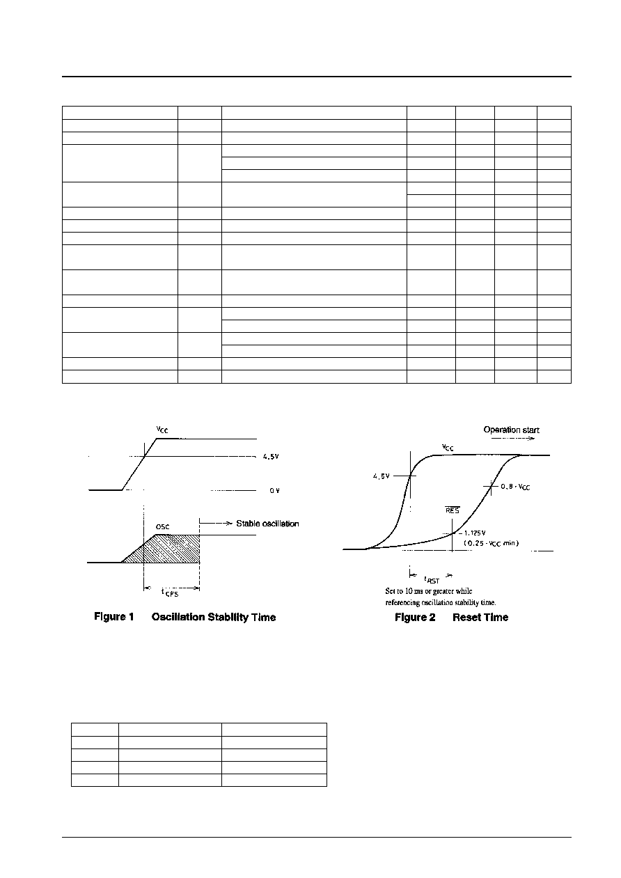
Ceramic oscillator stability time
t
CFS
Refer to Figure 1
10
ms
Reset time
t
RST
Refer to Figure 2
Note: 1. DATA START, DATA OUT, CLOCK OUT
2. RECEIVE, CORRECTION, ERROR, DATA START, DATA OUT, CLOCK OUT
Note: STK311-010 defaults to setting 1 though other settings are supported.
Other
The STK311-010 supports HIC internal settings for all output signals of CLK OUT and DATA START. These are
shown in the following table.
Table 1 Output Signal Settings
Setting
Polarity of CLK OUT
DATA START Output
1
Negative edge trigger
Every block
2
Negative edge trigger
Only 2nd block
3
Positive edge trigger
Every block
4
Positive edge trigger
Only 2nd block
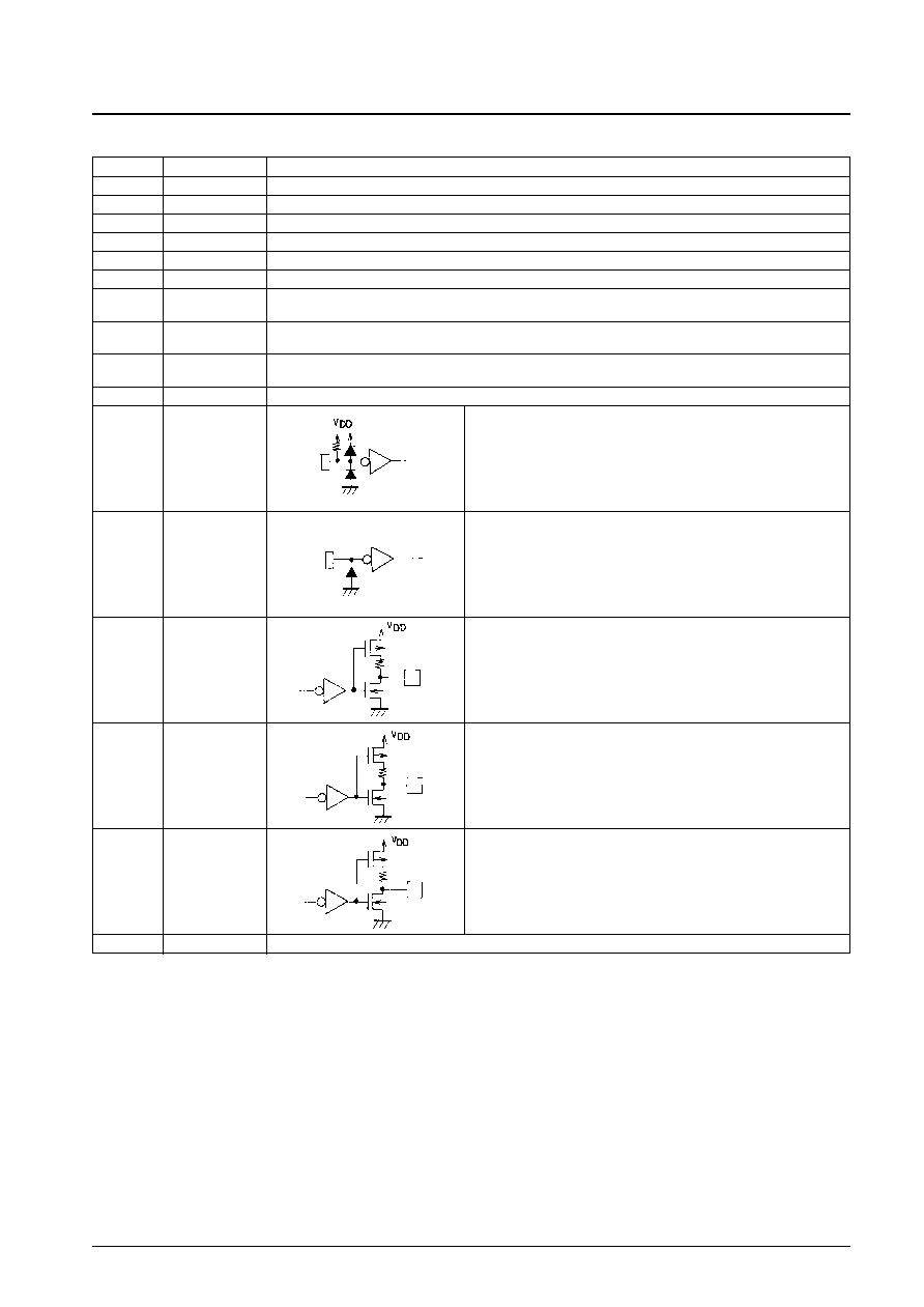
Internal Equivalent Circuit
No. 4374-3/7
STK311-010
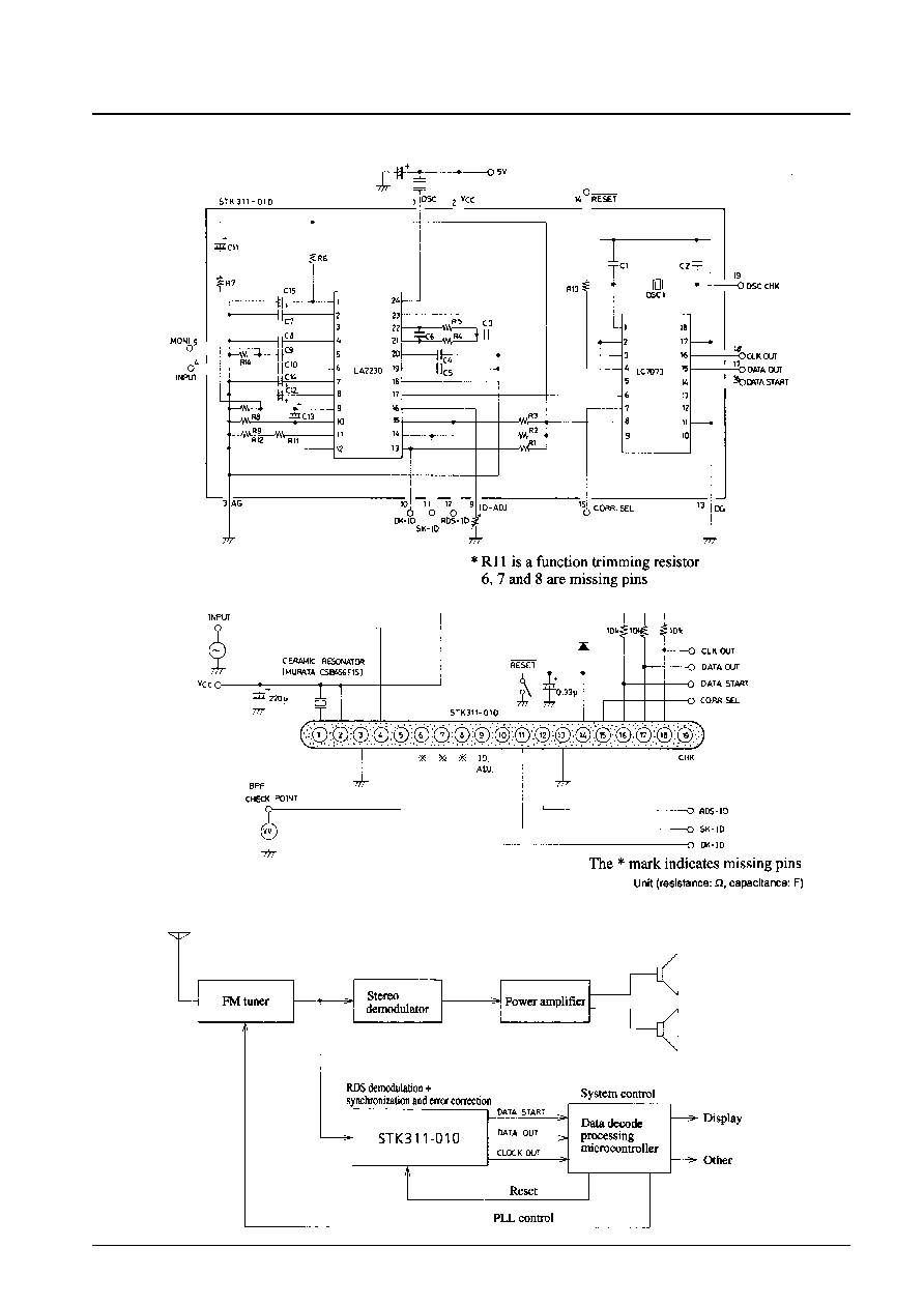
Sample System Configuration
Sample Application Circuit
No. 4374-4/7
STK311-010
Pin Functions
Pin No.
Pin name
Functions
1
OSC
This pin is for connecting the VCO ceramic oscillator (456 kHz).
2
V
CC
This power supply pin is for LA2230 and LC7073 plus power supply.
3
AG
This ground pin is for connecting the analog system (LA2230) ground (GND).
4
INPUT
This is the input pin.
5
MONI
This pin is for BPF (adjustment use) monitor output.
9
ID-ADJ
This pin is for SK detection sensitivity adjustment use.
10
DK-ID
Output pin for signaling existence of DK signal detection. When DK signal detection is possible, a low level output
is enabled and when detection is not possible, a high level is established.
11
SK-ID
Output pin for signaling existence of SK signal detection. When SK signal detection is possible, a low level output is
enabled and when detection is not possible, a high level is established.
12
RDS-ID
Output pin for signaling existence of RDS signal detection. When RDS signal detection is possible, a low level
output is enabled and when detection is not possible, a high level is established.
13
DG
This ground pin is for connecting the digital system (LC7073) ground (GND).
This pin is for reset input.
Reset restart inputs a low level for more than 4 clock cycles.
Schmitt type with an on-chip pull-up resistor.
14
RESET
15
CORR. SEL
16
DATA START
17
DATA OUT
18
CLK OUT
19
OSC CHK
Pin for OSC 1 oscillation frequency check.
Select input pin for error correction existence. This pin is for setting whether
or not errors within RDS demodulation data are corrected or output as is.
When set to 0, the correction function is disabled; a setting of 1 enables
error correction. Error correction mode corrects up to 5 bits within 5 bit
distance.
Output configuration controlled from serial data output block data starting
signal DS control input.
CMOS type output pin with pull-up MOS transistor.
Serial data output data
CMOS type output pin with pull-up MOS transistor.
Clock output.
CMOS type output pin with pull-up MOS transistor.
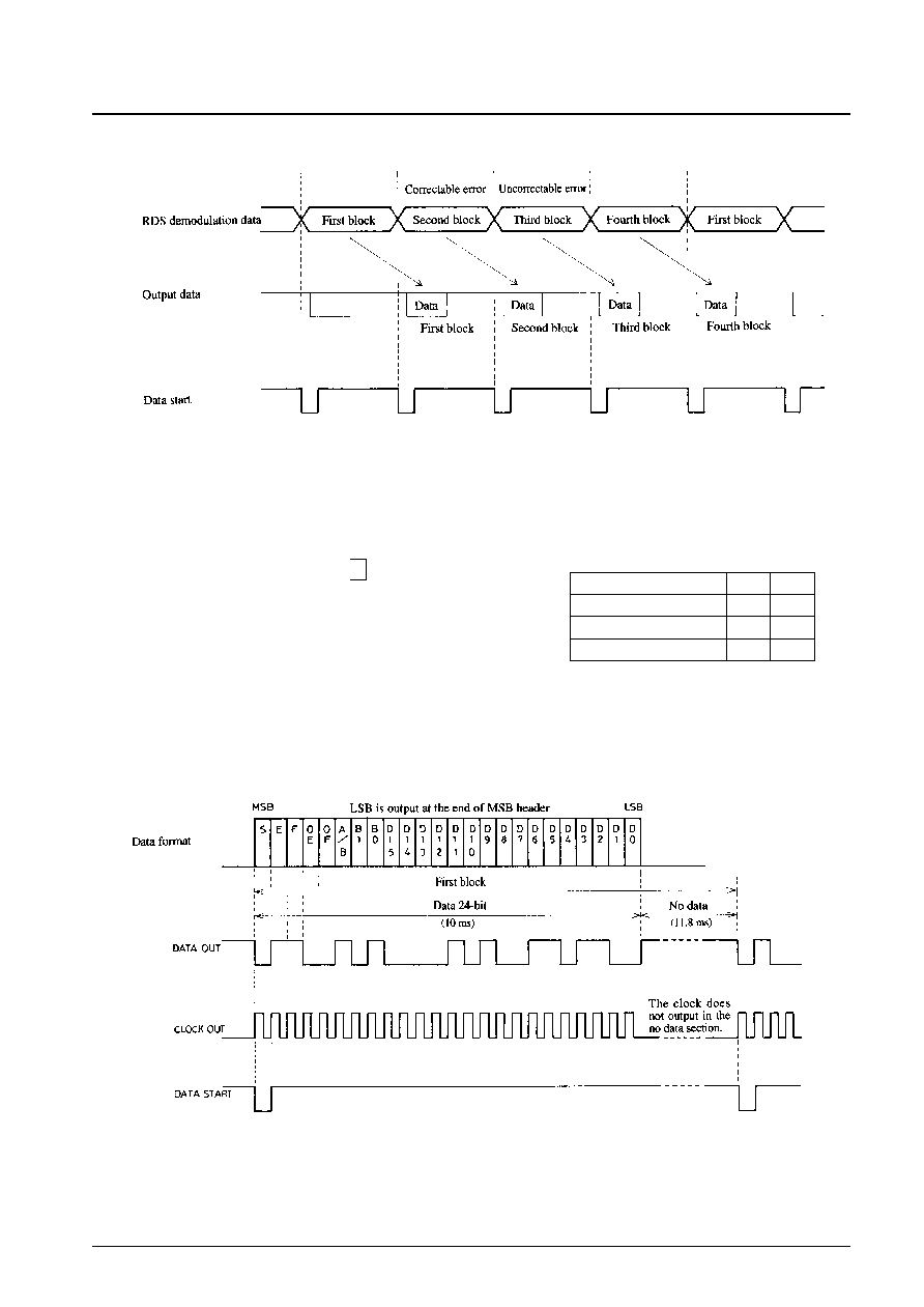
Relationship of RDS Demodulation Data (LA2230 Output) and LC7073 Output Data
∑ Serial data output from LC7073 (DATA OUT) is output 1 block slower
than data received from LA2230/2231.
Figure 3
Relationship of Demodulation Data and Output Data
Serial Data Output Format and Timing
S
: Start bit (defaults to 0)
E
: Error flag
Refer to table for flag settings
F
: Correction flag
OE
: Offset E (defaults to 0, future expansion use)
OF
: Offset F (defaults to 0, future expansion use)
A/B
: Group type version
0 : Version A
1 : Version B
B1 and B0
: Block number
00 : First block
01 : Second block
10 : Third block
11 : Fourth block
D15 to D0
: RDS data
Figure 4
Serial Data Output Format and Timing
No. 4374-5/7
STK311-010
Table 2 Error (E) and Correction (F) Flags
Item
E
F
No error
0
0
Correction complete
0
1
Uncorrectable
1
1