Thick Film Hybrid IC
Ordering number : EN4546A
N3096HA (OT)/83093YO 5-2308 No. 4546-1/3
SANYO Electric Co.,Ltd. Semiconductor Bussiness Headquarters
TOKYO OFFICE Tokyo Bldg., 1-10, 1 Chome, Ueno, Taito-ku, TOKYO, 110 JAPAN
AF Power Amplifier (Split Power Supply)
(60 W min, THD = 0.4%)
STK4038
II
Features
∑ Compact packaging supports slimmer set designs
∑ Series designed for 20 up to 200 W and pin-
compatibility
∑ Simpler heat sink design facilitates thermal design of
slim stereo sets
∑ The pulse noises associated with turning the power on
and off have been reduced by the adoption of fixed
current circuits
∑ Supports addition of electronic circuits for thermal
shutdown and load-short protection circuit as well as
pop noise muting which occurs when the power
supply switch is turned on and off
Package Dimensions
unit: mm
4033
Specifications
Maximum Ratings
at Ta = 25∞C
Parameter
Symbol
Condition
Rating
Unit
Maximum supply voltage
V
CC
max
±57
V
Thermal resistance
j-c
1.4
∞C/W
Junction temperature
Tj
150
∞C
Operating substrate temperature
Tc
125
∞C
Storage temperature
Tstg
≠30 to +125
∞C
Available time for load shorted
t
S
*
1
V
CC
= ±38 V, R
L
= 8
, f = 50 Hz, P
O
= 60 W
2
s
Recommended Operating Conditions
at Ta = 25∞C
Parameter
Symbol
Condition
Rating
Unit
Recommended supply voltage
V
CC
±38
V
Load resistance
R
L
8
Operating Characteristics
at Ta = 25∞C, V
CC
= ±38 V, R
L
= 8
, VG = 40 dB, Rg = 600
, R
L
(non-inductive)
Rating
Parameter
Symbol
Condition
min
typ
max
Unit
Quiescent current
I
CCO
V
CC
= ±45.5 V
10
20
50
mA
Output power
P
O
(1)
THD = 0.4%, f = 20 Hz to 20 kHz
60
W
P
O
(2)
V
CC
= ±32.5 V, THD = 1.0%, R
L
= 4
, f = 1 kHz
60
W
Total harmonic distortion
THD
P
O
= 1.0 W, f = 1kHz
0.3
%
Frequency response
f
L
, f
H
P
O
= 1.0 W, +0 dB
20 to 50k
Hz
≠3
Input resistance
r
i
P
O
= 1.0 W, f = 1kHz
55
k
Output noise voltage
V
NO
*
2
V
CC
= ±45.5 V, Rg = 10 k
1.2
mVrms
Neutral voltage
V
N
V
CC
= ±45.5 V
≠70
0
+70
mV
Note: Use rated power supply for test unless otherwise specified.
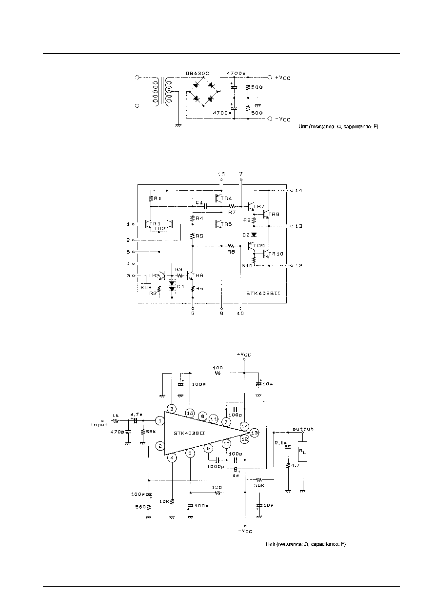
1. Use the transformer power supply shown on the next page when measuring the available time for load shorted and the output noise voltage.
2. Output noise voltage represents the peak value on the rms scale (VTVM). The noise voltage waveform does not include the pulse noise.
[STK4038II]

STK4038
II
No. 4546-3/3
This catalog provides information as of November, 1996. Specifications and information herein are subject to
change without notice.
s
No products described or contained herein are intended for use in surgical implants, life-support systems, aerospace
equipment, nuclear power control systems, vehicles, disaster/crime-prevention equipment and the like, the failure of
which may directly or indirectly cause injury, death or property loss.
s
Anyone purchasing any products described or contained herein for an above-mentioned use shall:
Accept full responsibility and indemnify and defend SANYO ELECTRIC CO., LTD., its affiliates, subsidiaries and
distributors and all their officers and employees, jointly and severally, against any and all claims and litigation and all
damages, cost and expenses associated with such use:
Not impose any responsibility for any fault or negligence which may be cited in any such claim or litigation on
SANYO ELECTRIC CO., LTD., its affiliates, subsidiaries and distributors or any of their officers and employees
jointly or severally.
s
Information (including circuit diagrams and circuit parameters) herein is for example only; it is not guaranteed for
volume production. SANYO believes information herein is accurate and reliable, but no guarantees are made or implied
regarding its use or any infringements of intellectual property rights or other rights of third parties.