 | –≠–ª–µ–∫—Ç—Ä–æ–Ω–Ω—ã–π –∫–æ–º–ø–æ–Ω–µ–Ω—Ç: STK4067 | –°–∫–∞—á–∞—Ç—å:  PDF PDF  ZIP ZIP |
Thick Film Hybrid IC
Ordering number : EN4376A
D3096HA (OT)/31293YO 5-2987 No. 4376-1/8
SANYO Electric Co.,Ltd. Semiconductor Bussiness Headquarters
TOKYO OFFICE Tokyo Bldg., 1-10, 1 Chome, Ueno, Taito-ku, TOKYO, 110 JAPAN
High-Output Power Amplifier
for Car Stereos (Po = 60 W typ.)
STK4067
Overview
Higher output amplification of the car stereo has been
generally dependent on boosting voltage of the power
supply. The STK4067 supports low-load impedance and
is designed for up to 60 W of high output without the
need for a power supply voltage booster circuit.
Applications
∑ Power amplifier for car stereos
∑ Home karaoke systems
∑ Radio-cassette players
Features
∑ Superior heat sink capacity using IMST (insulated
metal substrate technology)
∑ Designed for high output while supporting low-load
impedance
x R
L
= 1
60 W typ. (EIAJ)
100 W (max.)
R
L
= 2
40 W typ. (EIAJ)
70 W (max.)
z R
L
= 4
23 W typ. (EIAJ)
40 W (max.)
∑ Supports sufficient amplifier configurations for high
power output
∑ Low-load impedance driver
Supports independent or parallel speaker connections
for low-load impedance driving.
∑ Low distortion
THD = 0.025% typ. (V
CC
= 13.2 V, R
L
= 2
,
Po = 10 W, f = 1 kHz)
Compared with a monolithic IC, with a base
frequency of 100 Hz, the following is established:
secondary high frequency harmonics switches to
≠58 dB, with third-order switching to ≠20 dB,
fourth-order to ≠45 dB, and fifth-order to ≠18 dB.
∑ High temperature operation
Provides guaranteed high output to the passenger
compartments protected interior even when operating
in excessive heat
∑ Compact heat sink mounting
Supports compact total-set packaging, occupying 1/3
the heat sink area compared of monolithic ICs, and
equipped with an 85∞C temperature range and 110∞C
guaranteed case temperature rating
∑ Low operating power supply voltage range (9 V to 16 V)
∑ Built-in muting circuit
Short attack time with muting quickly enabled
∑ Built-in protection circuits
Built-in thermal shutdown and overvoltage protector
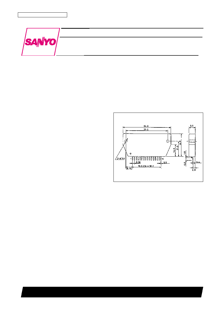
Package Dimensions
unit : mm
4131
[STK4067]
STK4067
No. 4376-2/8
Specifications
Maximum Ratings
at Ta=25∞C
Recommended Operating Conditions
at Ta=25∞C
Operating Characteristics
at Ta = 25∞C, V
CC
= 13.2 V, R
L
= 2
, Rg = 600
, VG = 46 dB
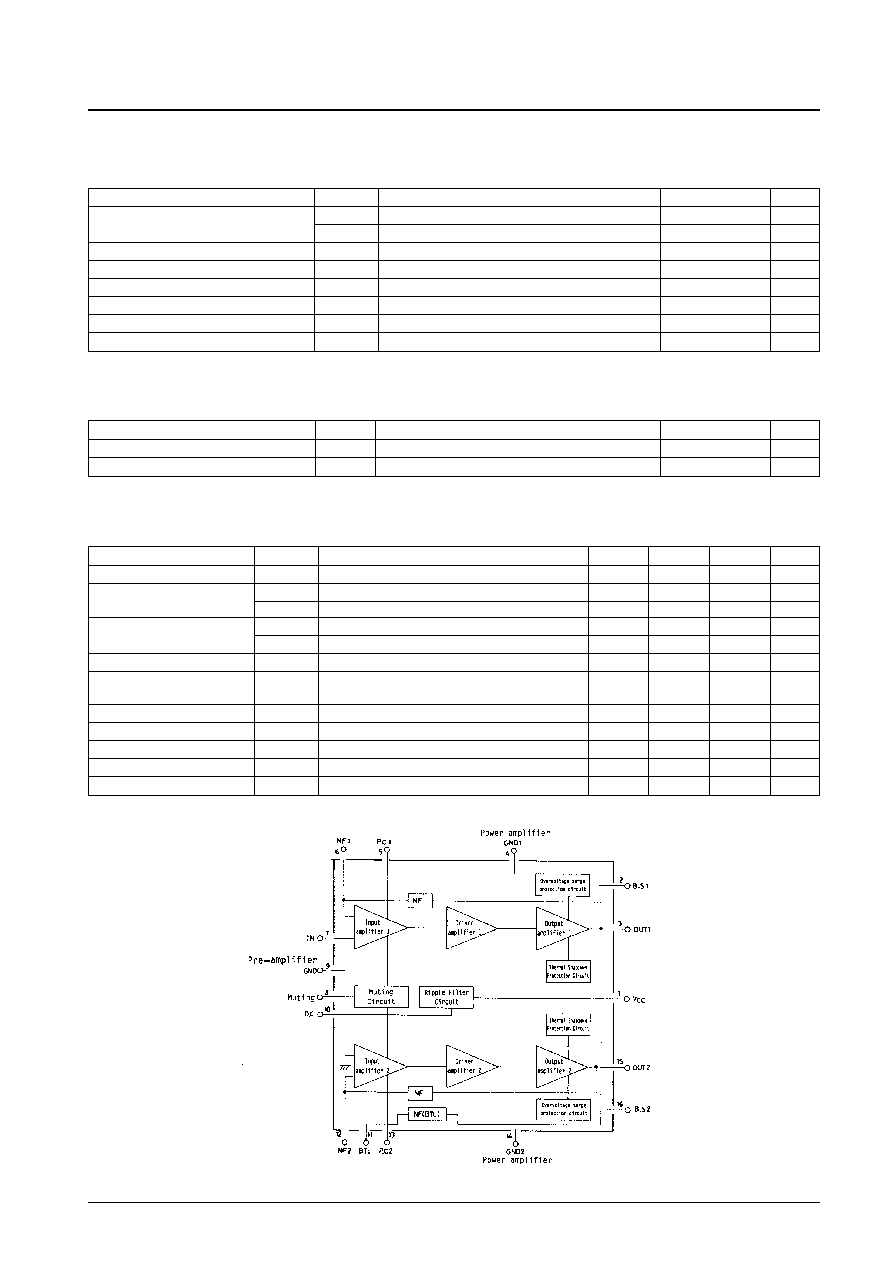
Equivalent Circuit
Parameter
Symbol
Conditions
Ratings
Unit
Maximum supply voltage
V
CC
max (1) No signal (with circuit cut off) 30s
30
V
V
CC
max (2) With signal (f = 100 kHZ, Vin = 1 Vrms, t = 100 ms)
18
V
Output current
I
O
max
15
A
Junction temperature
Tj
150
∞C
Thermal resistance
j-c
Per power transistor
1.6
∞C/W
Operating substrate temperature
Tc
110
∞C
Storage temperature
Tstg
≠40 to +125
∞C
Available time for load shorted
ts
V
CC
= 13.2 V, R
L
= 2
, f = 50 Hz, P
O
= 25 W
2
s
Parameter
Symbol
Conditions
Ratings
Unit
Recommended supply voltage
V
CC
13.2
V
Load resistance
R
L
2
Parameter
Symbol
Conditions
min
typ
max
Unit
Quiescent current
I
CCO
Rg = 10 k
70
140
mA
Output power
P
O
(1)
THD = 10%, f = 1 kHz, R
L
= 1
50
60
W
P
O
(2)
THD = 10%, f = 1 kHz, R
L
= 2
40
W
Total harmonic distortion
THD (1)
P
O
= 10 W, f =1kHz
0.025
0.1
%
THD (2)
P
O
= 1 W, f = 20 to 20 kHz
0.4
%
Voltage gain
VG
P
O
= 1 W, f = 1 kHz
43.8
46.0
48.2
dB
Frequency response
f
L
, f
L
P
O
=1 W,
+0
dB
20 to 30k
Hz
≠3
Input resistance
r
i
P
O
= 1 W, f = 1 kHz
20
30
k
Output noise voltage
V
NO
Rg = 10 k
, BPF
0.6
1.2
mVrms
Output offset voltage
VN
Rg = 10 k
≠200
0
+200
mV
Muting suppression level
ATT
V
M
= +5 V
dB
Ripple rejection
SVRR
f
R
= 100 Hz, Rg = 0
, V
R
= 0 dBm
≠47
dB

STK4067
No. 4376-3/8
STK4067 Design Data
(1) The Protection Circuits
a) Overvoltage Protector
Since the STK4067 is designed for car stereo applications, V
CC
max for operating mode is set to 18 V.
Exceeding the V
CC
maximum level activates the overvoltage protector and the circuit switches to an off-state and
delivers no output. The overvoltage protection circuit is set for a functional range from 18 to 28 V; 100%
operation at 28 V. For this reason, you should be careful not to exceed the 18 V limit in quiescent mode and keep
in mind AC line regulations when setting using a transformer power supply for designs such as home stereo
systems. Exceeding 18 V activates the overvoltage protector and results in the generation of abnormal sounds.
b) Thermal Shutdown
The thermal shutdown protection circuit is designed to first detect abnormal temperature rises which occur during
abnormal operation (such as load shorts) and then prevent damage to the IC by limiting the input signal; thereby
preventing a further rise in the temperature. The thermal shutdown protector is set to activate at substrate
temperature of 135∞C with a complete shutdown by switching to an off-state if temperatures rise to 175∞C. Under
normal application, the IC is equipped with a heat sink and the temperature never reaches a level resulting in a
complete off-state switch and saturation occurs at a specific temperature. For example, when a short occurs with
an IC mounted 4.5∞C/W heat sink, saturation is achieved at approximately 160∞C. At this point, Tj exceeds its
maximum rating of 170∞C. As previously mentioned, this circuit is designed to protect the IC from damage
sustained in a short period of time and you should note that the protection circuit will not protect the IC if
abnormal temperature rises occur over a long period of time.
(2) Precautions
a) Excessive Input
If a 1 V or greater (f = 1 kHz.rms) overinput is applied to the input pin, the DC balance of the input channel for
the input monolithic amplifier is disrupted and output is cut off. In addition, DC voltage is generated on the
output pins and causes damage to the speakers. Proper caution should be displayed in preventing input above this
voltage.
b) Parasitic Oscillation
The STK4067 performs phase compensation using 2.2
and 0.47µF between V
CC
and the bootstrap pins. Under
such conditions, the power supply line must be in a close proximity to the bootstrap pins for the inverting and
non-inverting amplifiers. If the power line is too long, parasitic oscillation is likely to occur at low temperatures.
If such a problem arises, add a 0.1µF rated condenser between the ground and the head of the power supply line
in order to lower the impedance.
c) Power Supply Voltage Inverse Application
The STK4067 is not equipped with a built-in power supply voltage inversion protection circuit. If the possibility
exists, one should be externally connected.
d) Power Off
Do not connect pin 1 of the V
CC
pin directly to the ground or else the IC will be damaged. When connecting pin
1, install a resistor rated for 100
or greater in series with pin 1, or you may place a diode between pin 10 and pin
1.
(3) Application Circuits
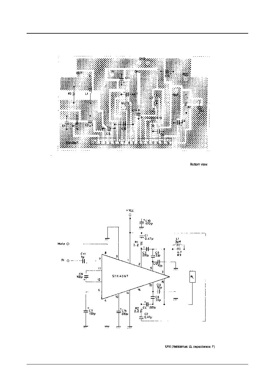
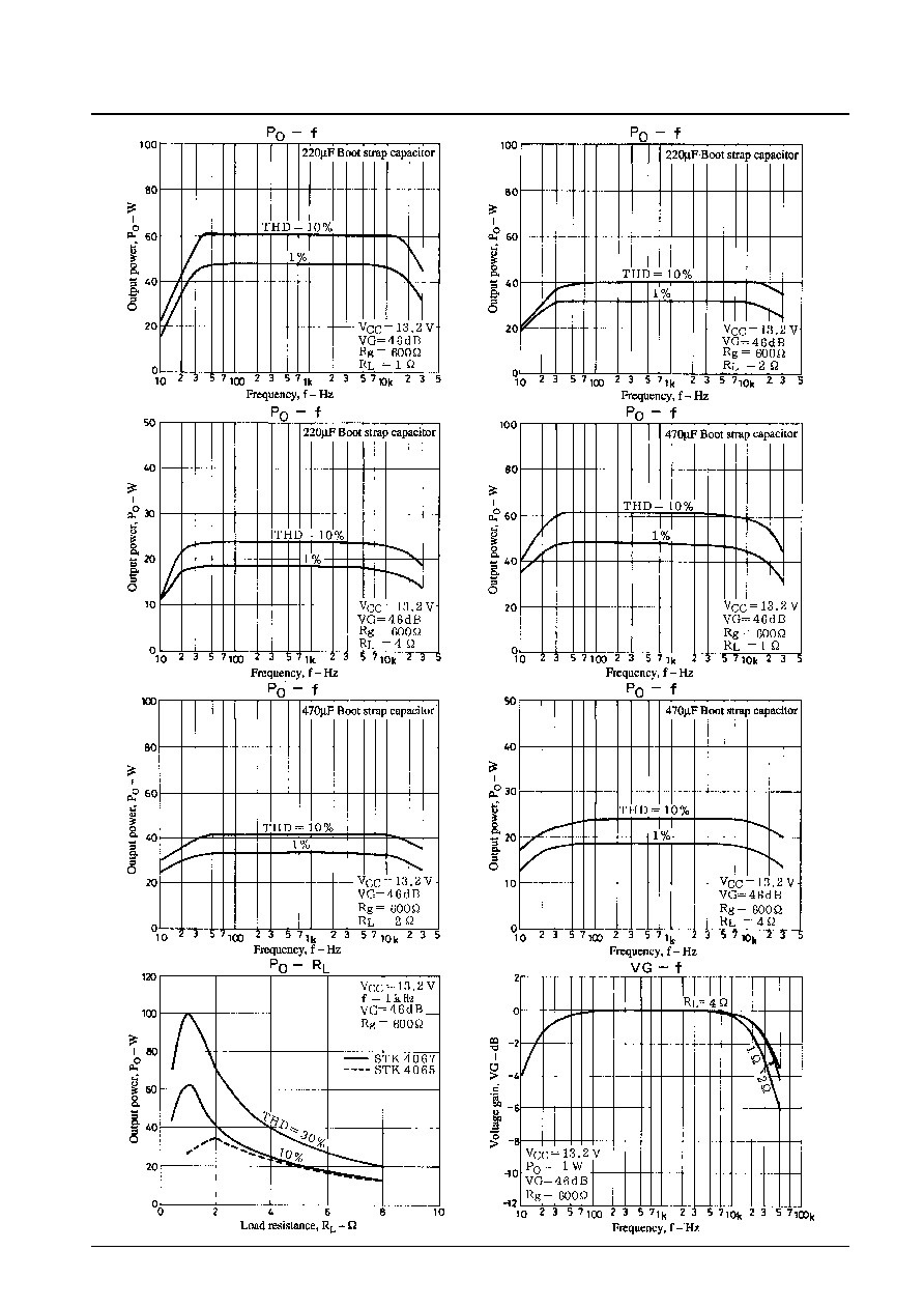
a) The under frequency band may be magnified, for applications using a booster amplifier or woofer driver
amplifier, the bootstrap condensers (C3 and C4) can be changed from 220µF to 470µF. Refer to P
O
-f graphs.
b) L1 = 3 µH and R3 = 4.7
are for anti-oscillation applications against capacity loads. We recommend the use of
this coil and resistor with the most compatible amplifier sets connected to general use speakers. This coil is not
necessary when the load capacity is low using a chosen speaker connected to a radio-cassette player or active
speaker.
STK4067
No. 4376-4/8
Example PCB
Sample Application Circuit

STK4067
No. 4376-5/8
Sample STK4067 Heat Sink Design
The radiator thermal resistance
c-a required for total substrate power dissipation Pd in the STK4067 is determined as:
Condition 1: IC substrate temperature Tc not to exceed 110∞C.
Pd
x
c-a+Ta <110∞C ∑∑∑∑∑∑∑∑∑∑∑∑∑∑∑∑∑∑∑∑∑∑∑∑∑∑∑∑∑∑∑ (1)
where Ta is set assured ambient temperature.
Condition 2: Power transistor junction temperature Tj not to exceed 150∞C.
Pd
x
c-a+Pd/N
x
j-c+Ta<150∞C∑∑∑∑∑∑∑∑∑∑∑∑∑(2)
where N is the number of power transistors and
j-c is the thermal resistance per power transistor chip.
However, power transistor power consumption is Pd equally divided by N units.
Expressions (1) and (2) can be rewritten based on
c-a to yield:
c-a<(110≠Ta)/Pd ∑∑∑∑∑∑∑∑∑∑∑∑∑∑∑∑∑∑∑∑∑∑∑∑∑∑∑∑∑∑∑∑∑∑∑∑∑∑(1)'
c-a<(150≠Ta)/Pd≠
j-c/N∑∑∑∑∑∑∑∑∑∑∑∑∑∑∑∑∑∑∑∑∑∑∑∑∑∑(2)'
The required radiator thermal resistance will satisfy both of these expressions.
From expressions (1)' and (2)', the required radiator thermal resistance can be determined once the following
specifications are known:
∑
Supply voltage
V
CC
∑
Load resistance
R
L
∑
Assured ambient temperature
Ta
The total substrate power consumption when STK4067 V
CC
is ±13.2 V and R
L
is 2
, for a continuous sine wave
signal, is a maximum of 19.3W (Fig. 2).
The STK4067 has four power transistors, so the thermal resistance per transistor
j-c is 1.6∞C / W. With an assured
ambient temperature Ta of 50∞C, the required radiator thermal resistance
c-a would be:
From expression (1)'
c-a <(110≠50)/19.3
<3.1
From expression (2)'
c-a <(150≠50)/19.3≠1.6/4
<4.78
To satisfy both, 3.1∞C/W is the required radiator thermal resistance.
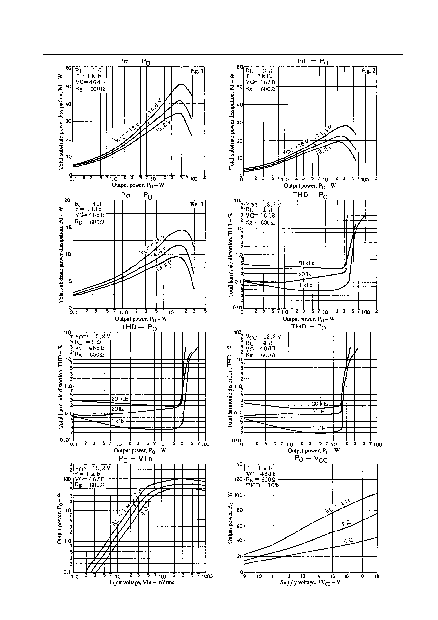
Figure 1 illustrates Pd - P
O
when the V
CC
of STK4067 is 13.2V and R
L
is functioning at 1
.
Pd max= 34.8W
From expression (1)'
c-a <(110≠50)/34.8
<1.72
From expression (2)'
c-a <(150-50)/34.8≠1.6/4
<2.47
To satisfy both, 1.72∞C/W is the required radiator thermal resistance.
Similar to figure 3 when the STK4067's V
CC
is 13.2 V and R
L
is 4
.
Pd max= 12W
From expression (1)'
c-a <(110≠50)/12
<5
From expression (2)'
c-a <(150-50)/12≠1.6/4
<7.93
To satisfy both, 5∞C / W is the required radiator thermal resistance. This design example is based on a fixed voltage
supply, and will require verification within your specific set environment.
STK4067
No. 4376-6/8
STK4067
No. 4376-7/8

STK4067
No. 4376-8/8
This catalog provides information as of December, 1996. Specifications and information herein are subject to
change without notice.
s
No products described or contained herein are intended for use in surgical implants, life-support systems, aerospace
equipment, nuclear power control systems, vehicles, disaster/crime-prevention equipment and the like, the failure of
which may directly or indirectly cause injury, death or property loss.
s
Anyone purchasing any products described or contained herein for an above-mentioned use shall:
Accept full responsibility and indemnify and defend SANYO ELECTRIC CO., LTD., its affiliates, subsidiaries and
distributors and all their officers and employees, jointly and severally, against any and all claims and litigation and all
damages, cost and expenses associated with such use:
Not impose any responsibility for any fault or negligence which may be cited in any such claim or litigation on
SANYO ELECTRIC CO., LTD., its affiliates, subsidiaries and distributors or any of their officers and employees
jointly or severally.
s
Information (including circuit diagrams and circuit parameters) herein is for example only; it is not guaranteed for
volume production. SANYO believes information herein is accurate and reliable, but no guarantees are made or implied
regarding its use or any infringements of intellectual property rights or other rights of third parties.