 | –≠–ª–µ–∫—Ç—Ä–æ–Ω–Ω—ã–π –∫–æ–º–ø–æ–Ω–µ–Ω—Ç: STK6103 | –°–∫–∞—á–∞—Ç—å:  PDF PDF  ZIP ZIP |
Thick-film Hybrid IC
Ordering number : EN4290A
73096HA (OT)/O012YO No. 4290-1/11
SANYO Electric Co.,Ltd. Semiconductor Bussiness Headquarters
TOKYO OFFICE Tokyo Bldg., 1-10, 1 Chome, Ueno, Taito-ku, TOKYO, 110 JAPAN
DC 3-phase Brushless Motor Driver
(Output Current 3A)
STK6103
Specifications
Maximum Ratings
at Ta = 25∞C
Allowable Operating Ranges
at Ta = 25∞C
Overview
The STK6103 is a hybrid IC incorporating a 3-phase
brushless motor controller and driver into a single
package, on the Sanyo IMST (Insulated Metal Substrate
Technology) substrate. Revolution speed is controlled
through the DC voltage level (Vref
1
) external input and
PWM control of motor phase winding current. The
driver is MOSFET to minimize circuit loss and handle
high-output current (rush current) demands.
Applications
∑ PPC and LBP drum motors
∑ Air conditioner fan motors
Features
∑ The output driver transistor is MOSFET for low power
loss (half that of a bipolar transistor) and reliable
handling of high-output current (rush current).
∑ Variation in Vref
1
level causes the driver transistor to
switch to PWM drive for high-efficiency motor speed
variation.
∑ Normal and reverse revolution select function.
∑ Start/stop and brake functions.
∑ Current limiter function.
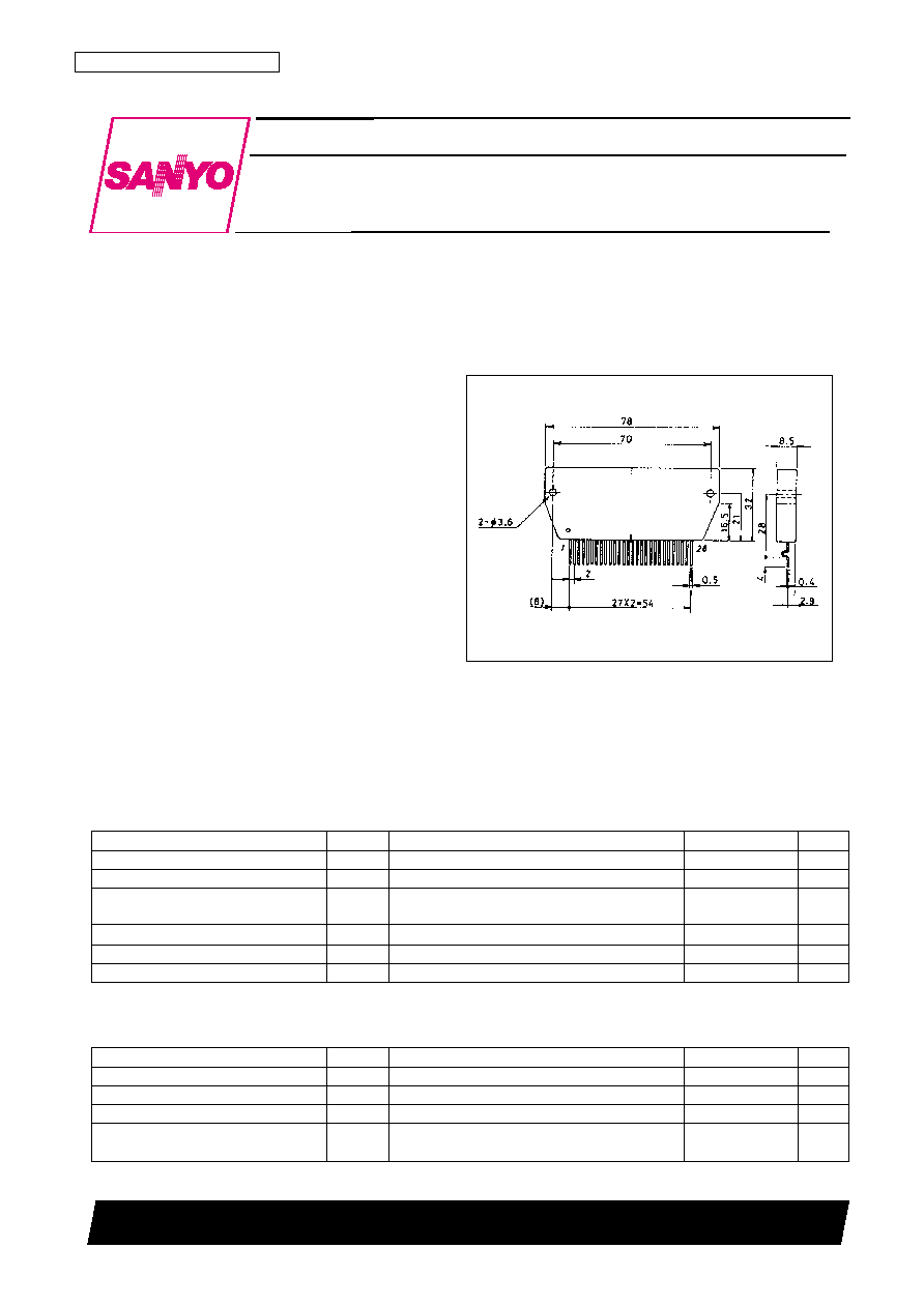
Package Dimensions
unit: mm
4130
[STK6103]
Parameter
Symbol
Conditions
Ratings
Unit
Maximum supply voltage 1
V
CC
1 max
No input signal
50
V
Maximum supply voltage 2
V
CC
2 max
No input signal
7
V
Maximum output current
I
O
max
Position detect input signal cycle = 30 ms,
5
A
PWM duty = 50%, operation time 1s
Operating substrate temperature
T
C
max
105
∞C
Junction temperature
T
j
max
150
∞C
Storage temperature
Tstg
≠40 to +125
∞C
Parameter
Symbol
Conditions
Ratings
Unit
Supply voltage 1
V
CC
1
With input signal
16 to 42
V
Output current
Io ave
DC phases present
3
A
Supply voltage 2
V
CC
2
With input signal
4.75 to 6.0
V
Brake current
I
OB
80 Hz full sine waves (all phases).
8
A
Operating time 0.1 s duty = 5% (see Note 1).
STK6103
No. 4290- 2/11
Electrical Characteristics
at Tc=25∞C, V
CC
1 = 24 V, V
CC
2 = 5.0 V
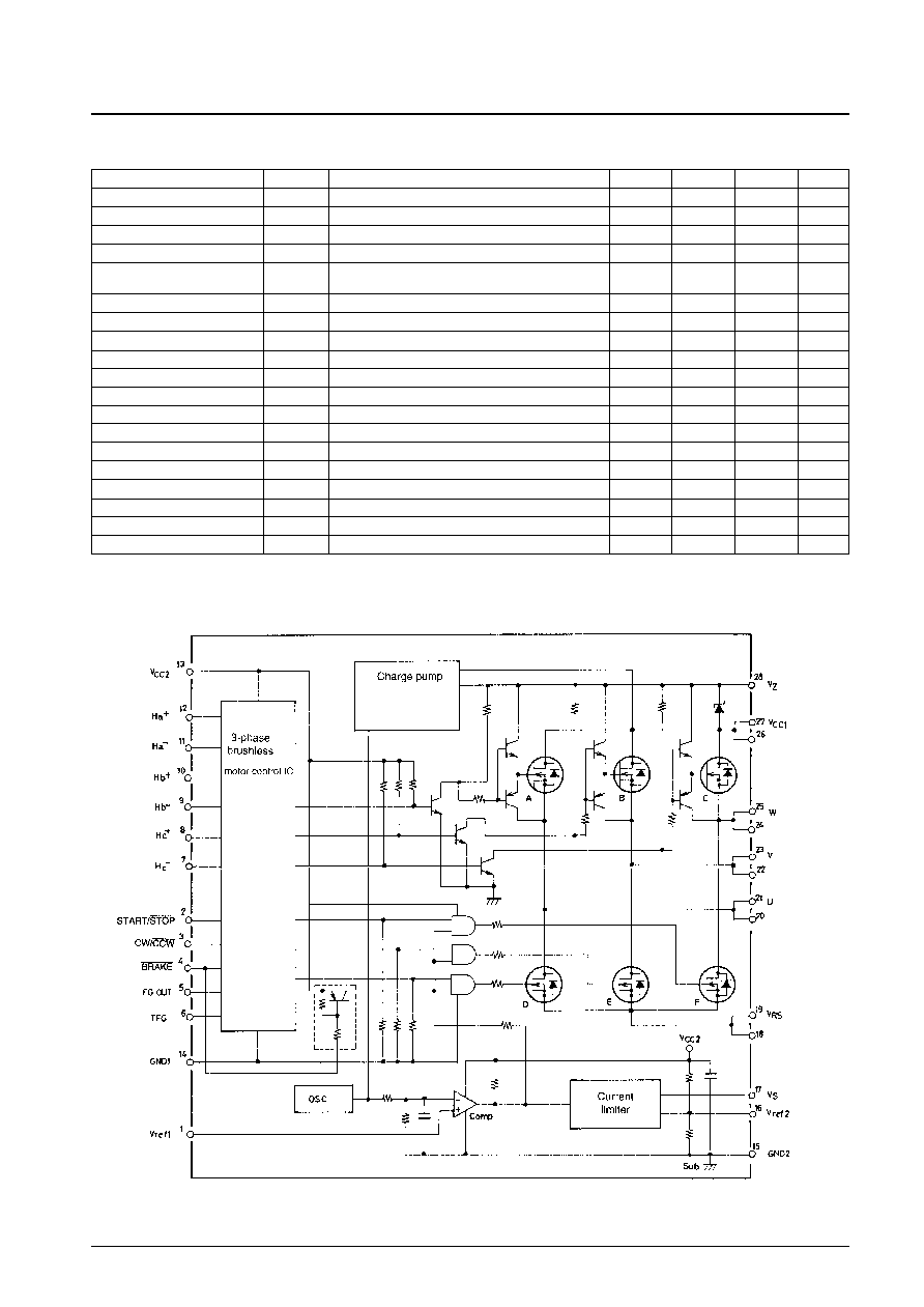
Equivalent Circuit
Parameter
Symbol
Conditions
min
typ
max
Unit
Supply current 1 (pin 13)
I
CCO
1
CW revolution
12
20
mA
Supply current 2 (pin 13)
I
CCO
2
Braking
26
38
mA
Output saturation voltage 1
Vst1
V
CC
1 side TR, Io = 3A
0.43
0.56
V
Output saturation voltage 2
Vst2
GND side TR, Io = 3A
0.47
0.62
V
Internal MOSFET diode
V
F
I
F
= 3A
0.95
1.5
V
forward voltage
PWM oscillation frequency
f
C
20
25
30
kHz
Current limiter reference voltage
Vref
2
0.47
0.50
0.53
V
Position detect input sensitivity
V
H
20
500
mV
Position detect common mode range
CMRH
2.0
4.5
V
Input "L" current 1 (pins 2,3)
I
IL1
V
IL1
= GND
130
200
µA
Input "L" voltage 1 (pins 2,3)
V
IL1
1.0
V
Input "L" current 2 (pin 4)
I
IL2
V
IL2
= GND
570
910
µA
Input "L" voltage 2 (pin 4)
V
IL2
1.0
V
Vref1 "H" voltage
Vref
1H
GND side transistor not in PWM
2.82
3.2
V
Vref1 "L" voltage
Vref
1L
GND side transistor off
0.15
0.35
V
Zener voltage
V
Z
5.7
6.2
6.7
V
FG output current
I
FGH
V
FG
= 1.6 V
80
µA
FG output "L" voltage
V
FGL
I
FG
= 0.3 mA
0.4
V
FG output pulse width
FG
C
F
= 0.1µF, R
F
= 10 k
0.9
1.0
1.1
ms
STK6103
No. 4290- 3/11
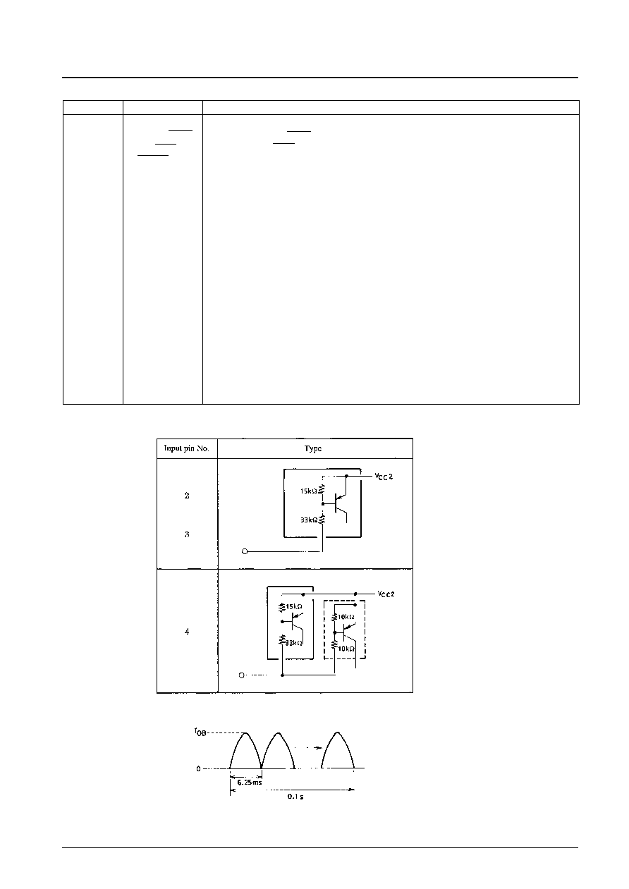
Pin Functions
Pin No.
Symbol
Function
1
Vref
1
GND-side driver transistor PWM control pin: range 0.15 to 3.2V
2
START/STOP
"H" = START, "L" = STOP (all transistors off)
3
CW/CCW
"H" = CW, "L" = CCW
4
BRAKE
"H" = rotate, "L" = Only GND-side transistor on
5
FG OUT
Position detect signal: output 6 pulses per cycle
6
TFG
For setting FG OUT "L" level pulse width. R
F
and C
F
pins.
7
H
C≠
Motor position detect signal input pin (to Hall device)
8
H
C+
Motor position detect signal input pin (to Hall device)
9
H
b≠
Motor position detect signal input pin (to Hall device)
10
H
b+
Motor position detect signal input pin (to Hall device)
11
H
a≠
Motor position detect signal input pin (to Hall device)
12
H
a+
Motor position detect signal input pin (to Hall device)
13
V
CC
2
Motor controller supply voltage pin
14
GND1
Motor controller IC GND pin: signal ground (SG)
15
GND2
External R
S
GND-side connection pin: power ground (PG)
16
Vref
2
Current limiter set pin: 0.1V
CC
2 when open
17
V
S
External R
S
current limiter detect pin
18, 19
V
RS
External R
S
connect pin
20, 21
U
Output pin (to motor winding)
22, 23
V
Output pin (to motor winding)
24, 25
W
Output pin (to motor winding)
26, 27
V
CC
1
Supply voltage pin (to motor)
28
VZ
Zener voltage (6.2V typ) for V
CC
1 driver transistor date source supply
Input Type
Note 1:
I
OB
indicates the operating current waveform peak as shown below.
STK6103
No. 4290- 4/11
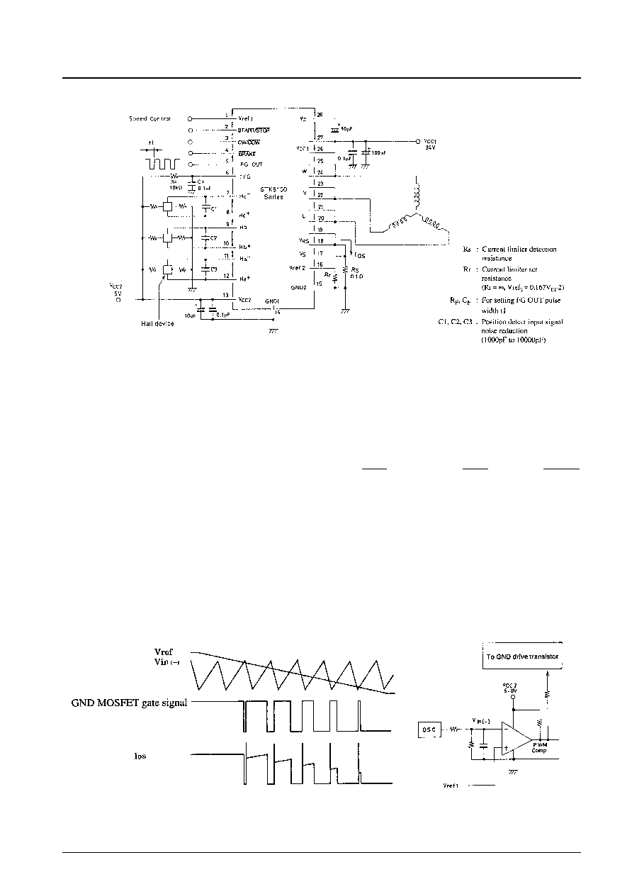
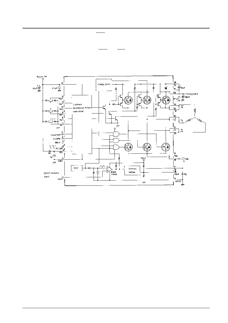
Sample Application Circuit
Description of Operation
The DC 3-phase brushless motor generally uses a permanent magnet for the rotor and places the stator coil around it.
When the rotor and stator coil are excited, magnetic force is generated between the poles, which is used for revolution
torque. For efficient revolution it is necessary to know precisely where the rotor pole is in relation to the stator pole. In
the brushless motor Hall devices and Hall ICs are widely used for this purpose, by detecting the electric power generated
along the lines of magnetic force.
(1)
Motor rotating force
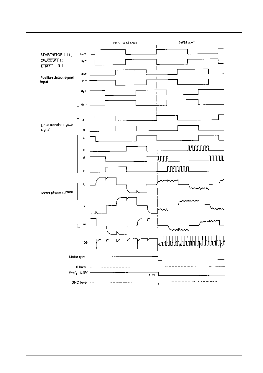
The block diagram for this HIC is given in Fig. 2.
The conditions before input of V
CC
1, with V
CC
2 on, are START/STOP pin H level, CW/CCW pin H level, BRAKE
pin H level and Vref
1
pin (speed control input) H level. The position detect signal at this time, due to the effect of
the rotor magnetic field, will be output signals from 1 or 2 devices (of the 3) so that H
X+
>H
X≠
is input to HIC pins 7
to 12. The signals input to pins 7 to 12 are input to the motor controller and converted into signals compatible with
3-phase brushless motor revolution. When V
CC
1 is supplied the charge pump circuit activates, generating V
CC
1
MOSFET gate voltage V
Z
. This outputs excitation current to the motor phase windings as indicated in the timing
chart (Fig. 3), and rotating the motor.
For revolution speed control, the Vref
1
pin voltage is converted and used for PWM drive to increase GND transistor
efficiency, controlling the conduction of motor current Io (Fig. 1). Control of Io means control of power supplied
to the motor, which controls motor rpm. In general motor rpm N is proportional to the PWM on duty (when motor
load is constant). The PWM on duty is proportional to the size of Vref
1
(see Fig. 13), and the relation of N is as
outlined below.
PWM ON Duty
Vref
1
Fig.1 PWM Drive Principle
STK6103
No. 4290- 5/11
Motor revolution is stopped by setting START/STOP to L level to turn off all drive transistors, and cut the supply of
current to the motor. Motor inertia will prevent instantaneous stopping. The brake function works to shorten the amount
of time needed to come to a complete stop. In input level L the V
CC
1 driver transistor is turned off, all GND driver
transistors are turned on, and the amount of power generated by the rotating motor windings reduced to reduce the rpms.
This brake function has priority over all START/STOP, CW/CCW and position detect input conditions.
Fig. 2 Block Diagram
STK6103
No. 4290-6/11
Fig. 3 I/O Timing Chart
STK6103
No. 4290-7/11
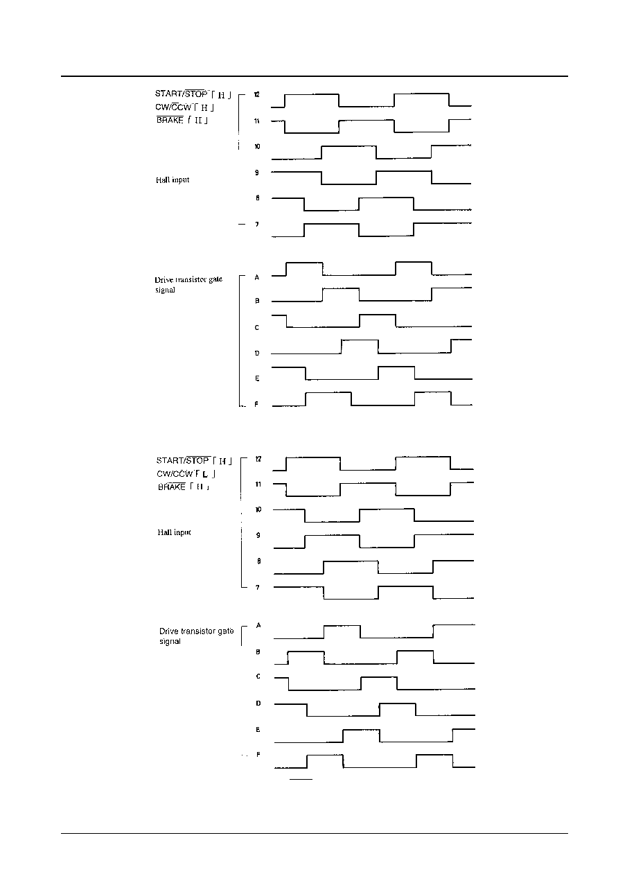
(2)
Other functions
CW/CCW
The direction of motor revolution can be selected by setting the input level to H or L. CW is H level and
CCW is L level. The CW timing chart is indicated in Fig. 3, and the CCW timing chart in Fig. 5.
Current limiter function
The current limiter converts the GND driver transistor source current into V
RS
through the external R
S
, and
controls GND driver transistor conduction based on a comparison of this voltage to Vref
2
. Vref
2
generates a
0.1 V
CC
2 voltage in pin open state. Vref
2
is generated by the voltage division between 27 k
and 3 k
resistances, and so the Vref
2
level can be readily reduced by attaching an external resistor. To prevent HIC
destruction in the event of motor lock, a current limiter can be enabled by setting Vref
2
at or below Io ave. If
no such protection is required, set Vref
2
between Io max and Io ave to limit rush current.
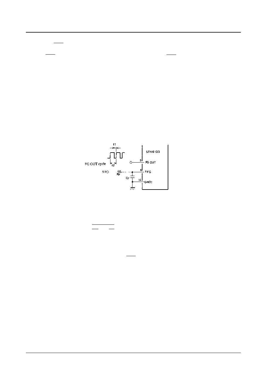
FG OUT
This pin outputs a square wave pulse proportional to one motor revolution, which can be used as the motor
servo-control PLL IC FG input signal. The square wave L level time t
1
is set by the time constant of C
F
and
R
F
connected to the TFG pin (Fig. 4).
Fig. 4
In general, when the n-pole 3-phase brushless motor fixed-speed rpm is expressed as N(rpm), the setting for t
1
so that t
1
= 0.5 t
2
is given by expression x.
t
1
=
1000
x
0.5
[ms]∑∑∑∑∑∑∑∑∑∑∑∑∑∑∑∑∑∑∑∑∑∑∑∑∑∑∑∑∑∑∑∑∑∑∑∑ x
N
x
6
x
n
60
2
The relation between C
F
, R
F
and t
1
is given by expression y.
t
1
a∑R
F
∑C
F
∑∑∑∑∑∑∑∑∑∑∑∑∑∑∑∑∑∑∑∑∑∑∑∑∑∑∑∑∑∑∑∑∑∑∑∑∑∑∑∑∑∑∑∑∑∑∑∑∑∑∑∑∑∑∑∑∑∑∑∑∑∑∑∑∑ y
However, a = 1
(
s
)
, R
F
= 3 k
to 30 k
, t
1
>50 µs
∑F
Expression x is designed to be half that of fixed speed t
2
, but when an FV conversion circuit is connected to
the FG OUT pin, it is necessary to reduce the duty to under 50%. In this case, adjust R
F
or C
F
as needed.
(3)
Precautions in drive
Start current (rush current)
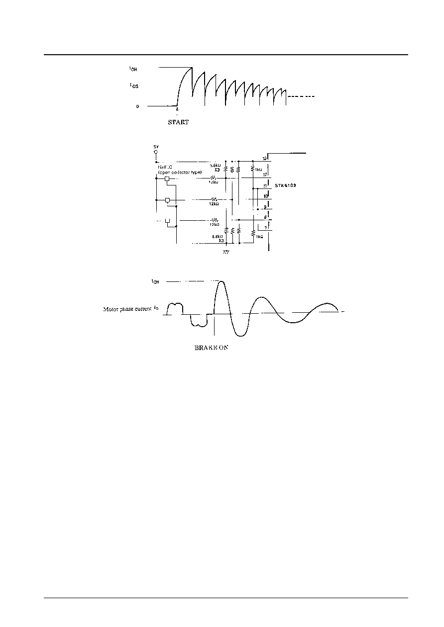
The motor start Rs current waveform is shown in Fig. 6. Current peak I
OH
must not exceed Io max.
Position detect signal
Because signal input sensitivity V
H
is ±500 mV max, the level of the output signal (open collector) from the
Hall IC must be reduced through conversion. A sample of this circuit is shown in Fig. 7. The position detect
signal must be compatible with the motor phase winding even in the time chart state shown in Fig. 3, or the
motor may not revolve smoothly.
Motor phase winding current during braking
The motor phase winding current during braking must not exceed Io max even during peak, although several
times set current levels are input.
STK6103
No. 4290-8/11
Fig. 5 CW/CCW I/O Timing Chart
STK6103
No. 4290- 9/11
Fig.6 Starting Current
Fig.7 Conversion Circuit for Hall IC and Hall Device Signal
Fig.8
Thermal Radiation Design
(1)
Internal average power dissipation Pd
The driver transistors represent the majority of the power dissipation in operation. Other losses are V
CC
2 and
the charge pump circuit. In PWM drive in particular, the diode in the V
CC
1 transistor is being used as a
flywheel diode, increasing V
CC
1 transistor loss. When these are included, internal mean power dissipation is:
Pd = Io (Vst
1
+ V
F
d
2
+ Vst
2
d
1
) + Pd
A
+ Pd
B
+ Pd
C
∑∑∑∑∑∑∑∑∑∑∑∑∑∑∑∑∑∑∑∑∑∑∑
Io
: Motor current
Vst
1
: V
CC
1 transistor saturation voltage
Vst
2
: GND transistor saturation voltage
d
1
: GND transistor PWM operation on duty
d
2
: GND transistor PWM operation off duty
Pd
A
: V
CC
2 loss
Pd
B
: Charge pump circuit loss
Pd
C
: GND transistor switching loss
V
F
: V
CC
1 transistor internal diode normal direction voltage
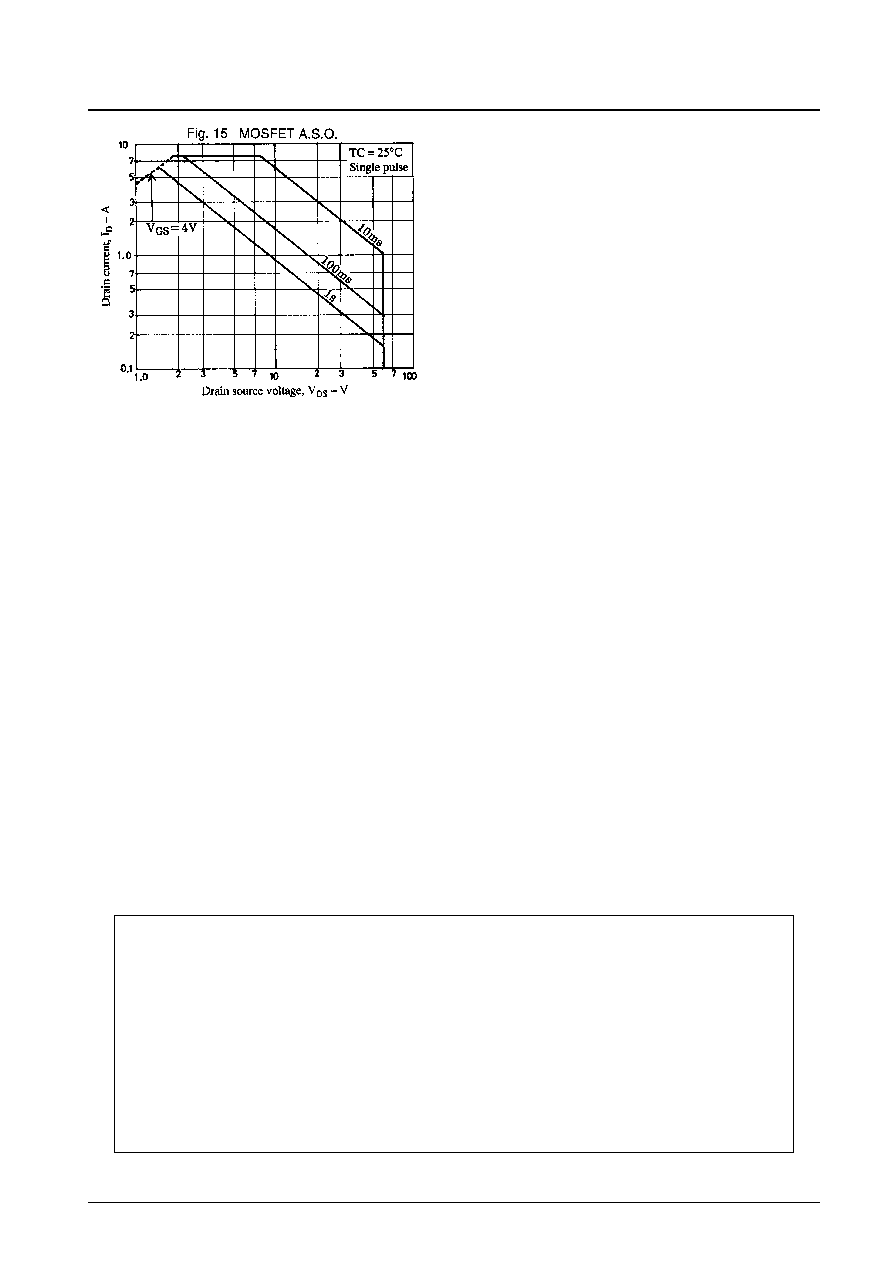
Because the driver transistor is a MOSFET, Vst
1
and Vst
2
will increase with an increase in I
O
or substrate
temperature Tc.
Pd
A
and Pd
B
are generally given as:
Pd
A
V
CC
2
x
I
CCO1
∑∑∑∑∑∑∑∑∑∑∑∑∑∑∑∑∑∑∑∑∑∑∑∑∑∑∑∑∑∑∑∑∑∑∑∑∑∑∑∑∑∑∑∑∑∑∑∑∑∑∑∑∑∑∑∑∑∑∑∑∑∑∑∑∑∑∑∑∑∑∑∑
Pd
B
V
CC
1
x
(0.49V
CC
1 ≠ 4.2)
x
0.001∑∑∑∑∑∑∑∑∑∑∑∑∑∑∑∑∑∑∑∑∑∑∑∑∑∑∑∑∑∑∑∑∑∑∑∑∑∑∑∑
where, V
CC
1 = 16 to 42V
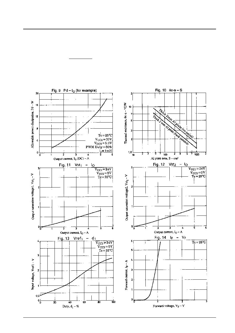
Refer to Figs. 11 to 14 for data on Vst
1
, Vst
2
, d
1
and V
F
.
STK6103
No. 4290- 10/11
(2)
Thermal radiation design
Actual thermal radiation design requires determination of the IC internal average power dissipation Pd from the
motor phase current Io (Fig. 9). Pd is then used to determine the thermal resistance for the radiator from the
following expression.
c ≠ a =
Tc max ≠ Ta
(∞C/W)
Pd
where Tc max = 105∞C
Ta = ambient temperature
With a 2.0 mm radiation plate, the required area can be determined from Fig. 10. Note that substrate temperature
will vary widely with set internal air temperature, and Tc for the mounted state must be 105∞C max.
STK6103
No. 4290- 11/11
This catalog provides information as of November, 1997. Specifications and information herein are subject to
change without notice.
s
No products described or contained herein are intended for use in surgical implants, life-support systems, aerospace
equipment, nuclear power control systems, vehicles, disaster/crime-prevention equipment and the like, the failure of
which may directly or indirectly cause injury, death or property loss.
s
Anyone purchasing any products described or contained herein for an above-mentioned use shall:
Accept full responsibility and indemnify and defend SANYO ELECTRIC CO., LTD., its affiliates, subsidiaries and
distributors and all their officers and employees, jointly and severally, against any and all claims and litigation and all
damages, cost and expenses associated with such use:
Not impose any responsibility for any fault or negligence which may be cited in any such claim or litigation on
SANYO ELECTRIC CO., LTD., its affiliates, subsidiaries and distributors or any of their officers and employees
jointly or severally.
s
Information (including circuit diagrams and circuit parameters) herein is for example only; it is not guaranteed for
volume production. SANYO believes information herein is accurate and reliable, but no guarantees are made or implied
regarding its use or any infringements of intellectual property rights or other rights of third parties.