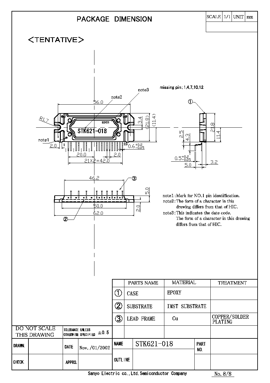
STK621-018
01.Nov.2002
Notes
Lower side It outputs FAULT signal with gate signal OFF.
However, it different from the protection operation of upper side, it is automatically reset
about 9 ms later and becomes an operation beginning condition when recovering to the normal
voltage. (The protection operation doesn't latch by the input signal.)
3.When assembling the hybrid IC on the heat sink, tightening torque range is 0.8Nm to 1.0Nm.
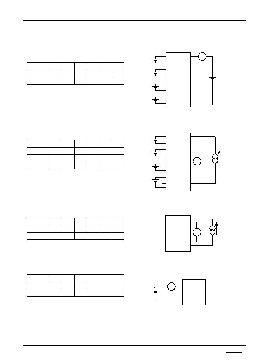
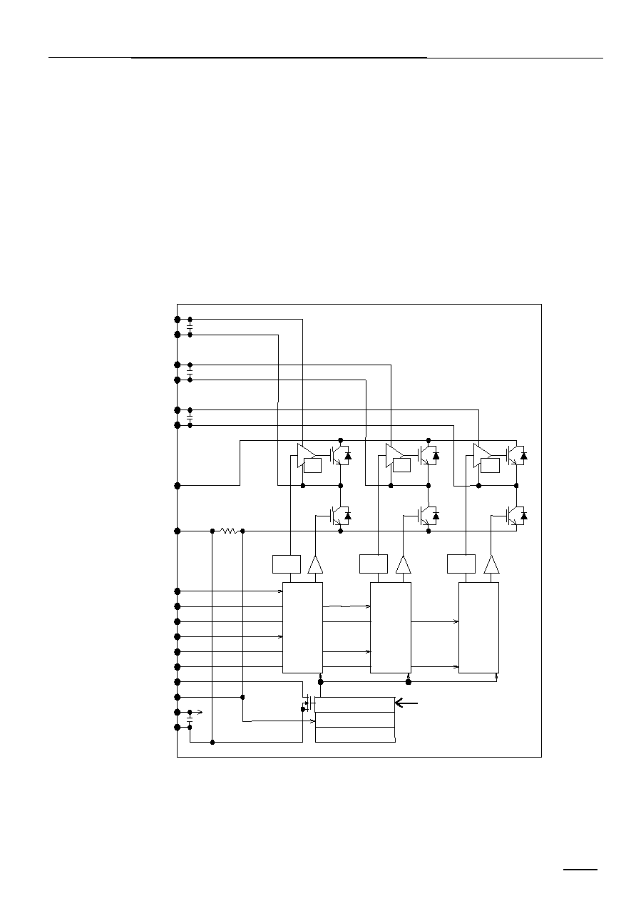
Circuit Block Diagram
V B1( 8)
U ( 9)
V B2( 5)
V ( 6)
V B3( 2)
W ( 3)
(11)
- (13)
H IN 1(14)
H IN 2(15)
H IN 3(16)
LIN 1(17)
LIN 2(18)
LIN 3(19)
Fault(20)
Iso 21)
V D D (22)
V ss(23)
Logic
Level
Shifter
Logic
Level
Shifter
Logic
Level
Shifter
C B
C B
C B
Shunt R esistor
Latch
O ver-C urrent
V D D -U nder V oltage
U .V .
U .V .
U .V .
Latch T im e A bout 9m s
( A utom atic R eset )
Electric Co.,Ltd. Semiconductor Company No.3/8

STK621-018
01.Nov.2002
Usage Precautions
1. By the addition of the diode for the bootstrap (DB : high speed type, withstand voltage equa
l to or more than 600V) and of the capacitor (CB : about 1 to 47F), a single power supply
drive is enabled. In this case, it makes a lower side IGBT ON (input signal of lower side
makes LOW). Then it charges in CB. Incidentally, in case of start-up and so on, when the
voltage of CB is low, the big charging electric current flows and sometimes becomes the
cause which exerts the bad influence of the noise and so on. Put limitation resistance RB
(Several to about tens of ). (When not using bootstrap circuit, each upper side
pre-drive power supply needs an independent power supply. Externally set.) Also, the upper
side power supply voltage sometimes declines by the way of controlling. Confirm it
2. Because the jump voltage which is accompanied by the vibration in case of switching
operation occurs by the influence of the floating inductance of the wiring of the outer
power supply which is connected with of the + terminal and the ≠ terminal, restrains and
spares serge voltage being as the connection of the snubber circuit (Capacitor / CS / about
0.1 - 10 F) for the voltage absorption with the neighborhood as possible between + and the
- terminal, and so on, with making a wiring length (among the terminals each from CI) short
and making a wiring inductance small.
3. Iso terminal (20pin) is for the electric current monitor. Be careful, because the
overcurrent protection does not operate when short-circuiting in the Iso terminal and the
Vss terminal.
4. Output form of the FAULT terminal is open DRAIN (it is operating as FAULT when becoming LOW).
When the pull up with the resistance, use above 5.6K.
5. The overcurrent protection feature operates only when it is possible to do a circuit control
normally. For the safety, put a fuse, and so on in the Vcc line.
6. Because the IC sometimes destroys and bursts when motor connection terminal (3pin,6pin,9pin)
becomes open while the motor turns, especially, be careful of the connection ( the soldering
condition ) of this terminal.
This data shows the example of the application circuit, does not guarantee a design as the mass.
Electric Co.,Ltd. Semiconductor Company No.7/8