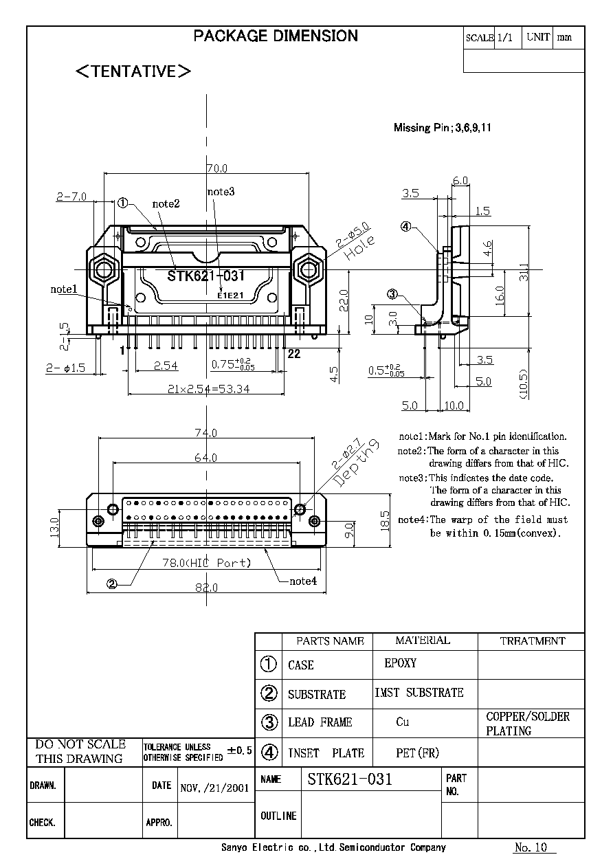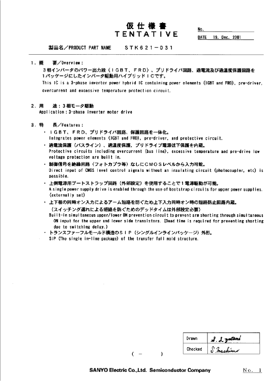
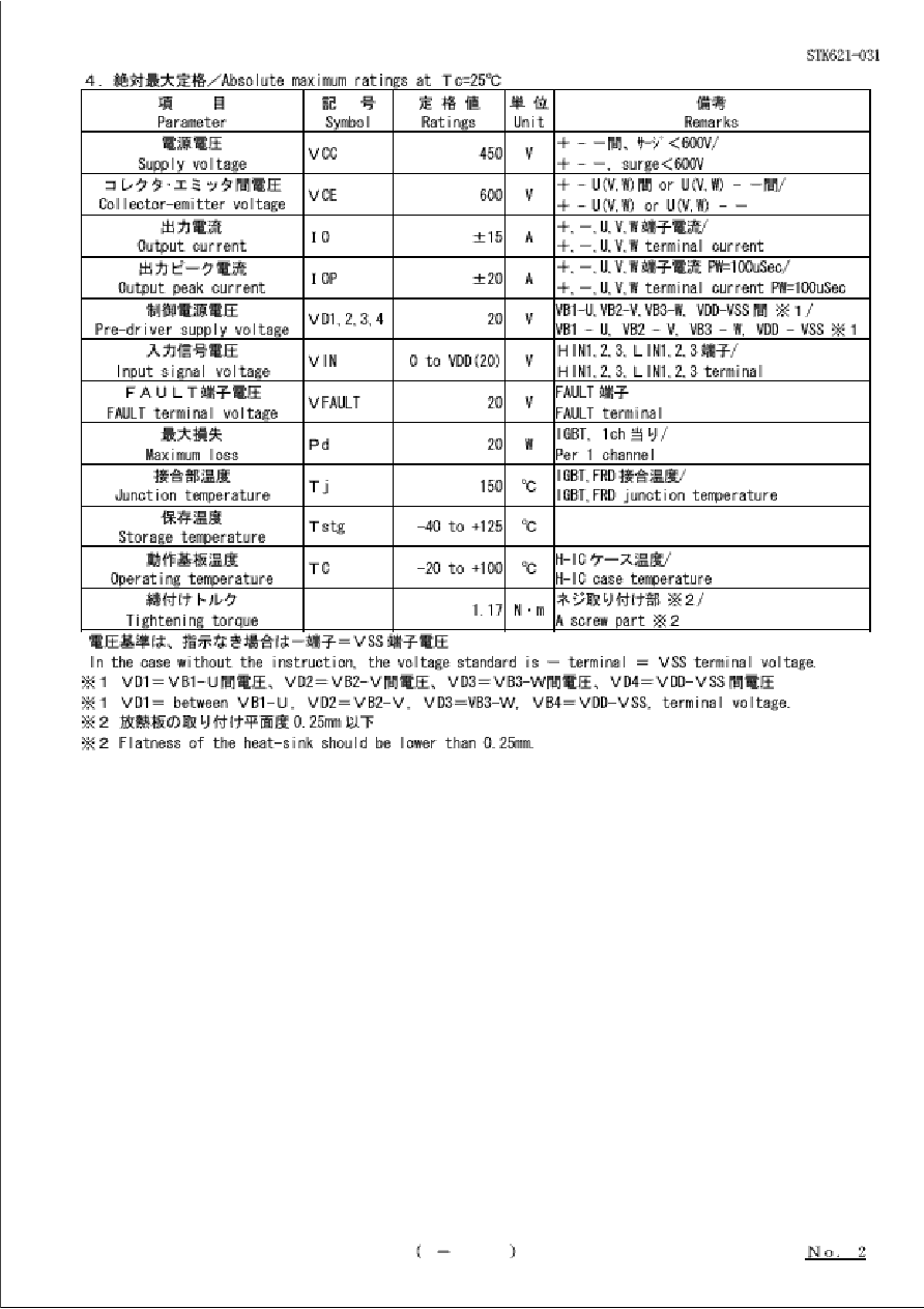
STK621-031
-
3
Electrical characteristics at c=25
∞C, D=15V
/Ratings
Parameters
Symbols
Conditions
Test
Circuit
Min. Typ. Max.
Unit
Power output part
Collector-to-emitter
cut-off current
CE CE=600V
1
Fig.1
≠
≠ 2
mA
Upper side
≠
1.6 2.2 V
Collector-to-emitter
saturation voltage
CE(SAT) O=7.5A
Lower side
2
Fig.2
≠ 1.8 2.4 V
Upper side
≠ 1.5 2.2 V
Diode forward voltage
F O=-7.5A
Lower side
3
Fig.3
≠ 1.7 2.4 V
j-c(T) IGBT
≠
≠ 4.5 ≠ ∞C/W
Junction-to-substrate
thermal resistance
j-c(D) FWD
≠
≠ 5.5 ≠ ∞C/W
Control (Pre-driver) part
D1,2,3=15V
≠ 0.05
≠
Pre-drive power supply
consumption electric
current
D
D4=15V
4
Fig.4
≠
10
≠
mA
ON
Input ON voltage
IH Output
ON
≠
≠
≠ 1.5 V
OFF
Input OFF voltage
IL Output
OFF
≠ 3.5
≠
≠ V
Protection part
Excessive temperature
SD
The substrate surface
≠
100
≠
120
Overcurrent protection
electric current
SD PW=100s
5
Fig.5
17
≠
24 A
Pre-drive low voltage
protection
VLO
≠
9
≠
12 V
Fault
Fault terminal input
electric current
OSD VFault=1.0V
≠
≠
2
≠
mA
ON
≠
1.0
≠ s
Switching time
OFF
O=7.5A, /
Inductive load
6
Fig.6
≠ 1.2 ≠ s
Electric current output
signal level
SO O=7.5A
≠
≠
0.18
≠
V
-SS
In the case without the instruction, the voltage standard is - terminal SS terminal voltage.

STK621-031
-
4
Notes
ON IGBT ON OFF IGBT OFF
ON IH(MAX)OFF IL(MIN)DD
Input ON voltage indicates a value to turn on output stage IGBT.
Input OFF voltage indicates a value to turn off output stage IGBT.
At the time of output ON, set the input signal voltage 0V to IH (MAX).
At the time of output OFF, set the input signal voltage IL (MIN) to DD.
( :)
()() s
When the internal protection circuit operates, there is FAULT signal ON (When the FAULT terminal is
low level, FAULT signal is ON state : output form is open DRAIN). It continues a latch if either of six
input signals is doing ON (Low level). A latch condition is reset about 10 s later after all six input
signals become OFF (High level).
(LO)
But, the operation of pre-drive power supply low voltage protection (UVLO) is as follows.
FAULT
(Low)
Upper side There is not FAULT signal output but it does a corresponding gate signal OFF.
Incidentally, it returns to the regular operation when recovering to the normal voltage
but the latch continues among input signal ON (Low).
FAULT
(
)
Lower side It outputs FAULT signal with gate signal OFF.
However, it different from the protection operation of upper side, it is automatically
reset and becomes an operation beginning condition when recovering to the normal voltage.
(The protection operation doesn't latch by the input signal.)
0.791.17
0.25mm
When assembling the hybrid IC on the heat sink, tightening torque range is 0.79Nm to 1.17Nm.
Flatness of the heat-sink should be lower than 0.25mm.
The pre-drive low voltage protection is the feature to protect a device when the pre-driver supply
voltage declines with the operating malfunction. As for the pre-driver supply voltage decline in
case of operation beginning, and so on, we request confirmation in the set.
STK621-031
-
5
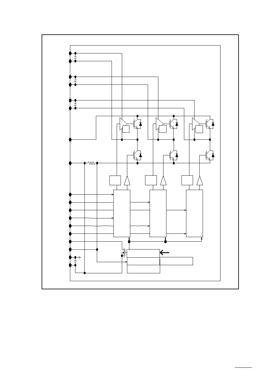
Internal equivalent circuit diagram
VB1( 1)
U( 2)
VB2( 4)
V( 5)
VB3( 7)
W( 8)
(10)
-(12)
HIN1(13
HIN2(14
HIN3(15
LIN1(16)
LIN2(17)
LIN3(18)
FAULT(19)
ISO(20)
VDD(21)
VSS(22)
Logic
Level
Shifter
Logic
Level
Shifter
Logic
Level
Shifter
CB
CB
CB
Shunt Resistor
Latch
Over - Current
VDD-Under Voltage
U.V.
U.V.
U.V.
Reset
( All input = High / OFF )
Over - temp.
STK621-031
-
6
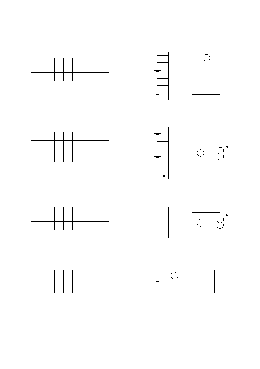
Test Circuit
V D 1 1 5 V
V D 2 1 5 V
V D 3 1 5 V
V D4 1 5V
V D 1 1 5 V
VD 2 15 V
V D3 1 5V
VD 4 15 V
F i g C E
F i g C E( SA T)
CE
CE
M
N
U+
10
2
V+
10
5
W+
10
8
U-
2
12
V -
5
1 2
W -
8
1 2
o
CE(SAT)
M
N
m
U+
10
2
13
V+
10
5
14
W+
10
8
15
U-
2
12
16
V -
5
1 2
1 7
W -
8
1 2
1 8
F i g F
M
N
U+
10
2
V+
10
5
W+
10
8
U-
2
12
V -
5
1 2
W -
8
1 2
F
o
F i g D
m
n
V D1
1
2
V D2
4
5
V D3
7
8
VD 4
21
22
D
D
STK621-031
-
7
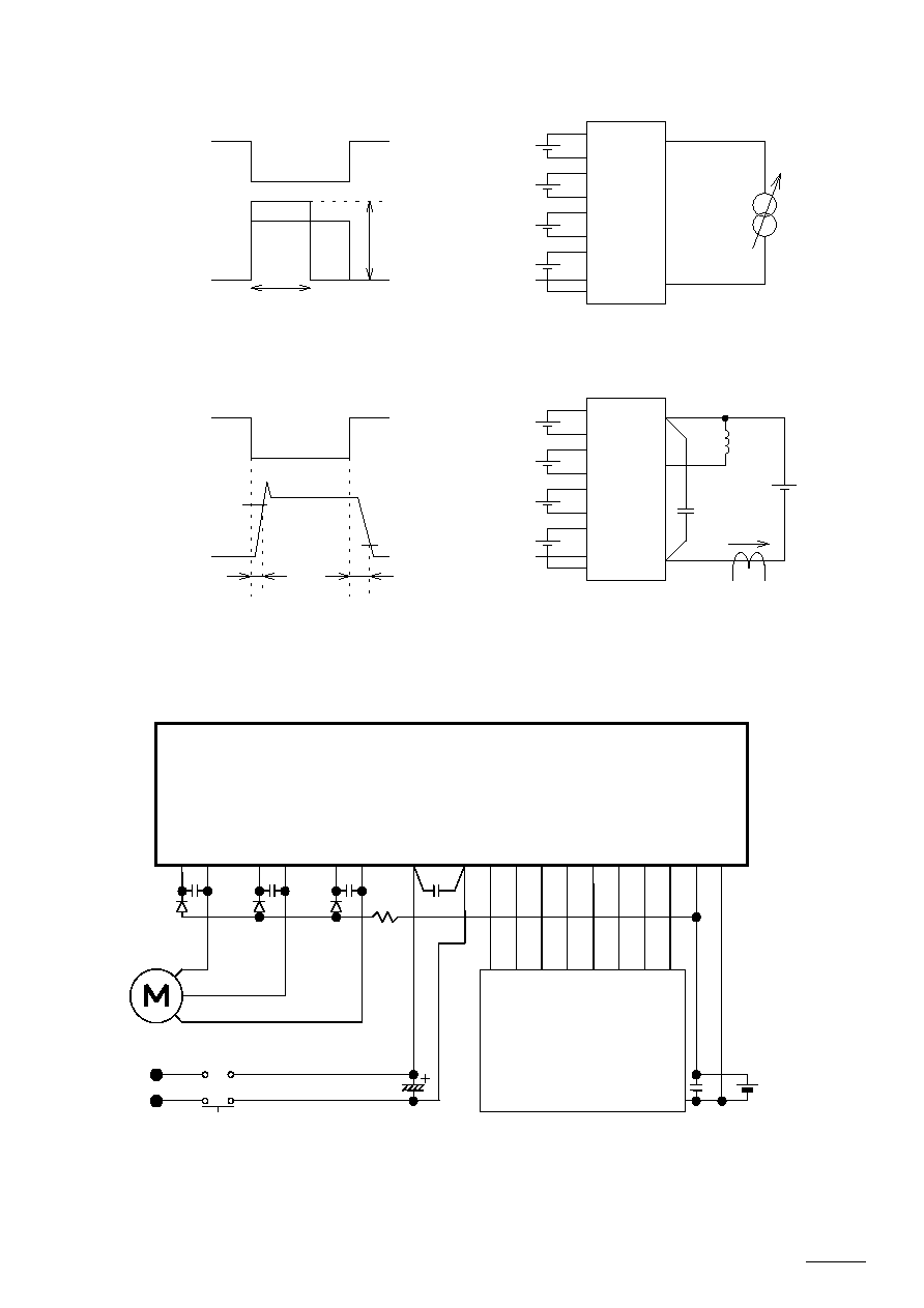
V D 1 1 5 V
V D 2 1 5 V
V D 3 1 5 V
V D 4 1 5 V
I n p u t s i g n a l
V D 1 1 5 V
V D 2 1 5 V
V D 3 1 5 V
V D 4 1 5 V
I n p u t s i g n a l
o
F i g S D
F i g S w i t c h i n g T i m e
I n p u t s i g n a l
o
S D
1 0 0 S
c c
o
I n p u t s i g n a l
o
O N
O F F
1 0
9 0
0 5
Example of the application circuit
1
2
4 5 7 8
10 12
13
14
15
16
17
18
19
20
21
22
Control Logic
VDD=15V
LIN3
LIN2
LIN1
HIN3
HIN2
HIN1
VDD
ISO
VSS
FAULT
-
VCC
CB
CB CB
DB
DB
DB
RB
CS
CI
STK621-031
CD
W
VB3
V
VB2
U
VB1
-
STK621-031
-
8
The Recommendation Operating Conditions
The Recommendation
Operating Conditions
Parameters
Symbol
Conditions
Min. Typ. Max.
Unit
Supply voltage
CC
- -
- -
0 280
400
D1,2,3
VB1 - U,VB2 - V,VB3 - W
VB1 - U,VB2 - V,VB3 - W
12.5 15 17.5
Pre-driver supply voltage
D4
VDD - VSS
VDD - VSS
13.5 15 16.5
ON
Input ON voltage
IN(ON)
0 - 1
OFF
Input OFF voltage
IN(OFF)
HIN1,HIN2,HIN3,
LIN1,LIN2,LIN3
HIN1,HIN2,HIN3,
LIN1,LIN2,LIN3 Terminal
4 5 VDD
frequency
PWM
1 - 10 KHZ
Deadtime
Upper/lower input signal downtime
2 - -
s
Tightening torque
`'Type Screw
0.79 - 1.17 Nm
VD4=15±1.5V O=20mA(DC),0.5A(Peak)
Pre-driver power supply (VD4=15±1.5V) must have the capacity of O=20mA(DC), 0.5A(Peak).
Usage Precautions
:DB( 600V trr )
CB(147F ) ON (
LOW) CB CB
RB()
By the addition of the diode for the bootstrap (DB : high speed type, withstand voltage equal to or more
than 600V) and of the capacitor (CB : about 1 to 47F), a single power supply drive is enabled. In
this case, it makes a lower side IGBT ON (input signal of lower side makes LOW). Then it charges in CB.
Incidentally, in case of start-up and so on, when the voltage of CB is low, the big charging electric
current flows and sometimes becomes the cause which exerts the bad influence of the noise and so on.
Put limitation resistance RB (Several to about tens of ). (When not using bootstrap circuit, each
upper side pre-drive power supply needs an independent power supply. Externally set.) Also, the upper
side power supply voltage sometimes declines by the way of controlling. Confirm it.
-
(CI )-
(/CS/0.110F )
Because the jump voltage which is accompanied by the vibration in case of switching operation occurs
by the influence of the floating inductance of the wiring of the outer power supply which is connected
with of the + terminal and the ≠ terminal, restrains and spares serge voltage being as the connection
of the snubber circuit (Capacitor / CS / about 0.1 - 10 F) for the voltage absorption with the neighborhood
as possible between + and the - terminal, and so on, with making a wiring length (among the terminals
each from CI) short and making a wiring inductance small.

STK621-031
-
9
Usage Precautions
SO (20pin)SO SS
SO terminal (20pin) is for the electric current monitor. Be careful, because the overcurrent protection
does not operate when short-circuiting in the SO terminal and the SS terminal.
FAULT (LOW FAULT )5.6K
Output form of the FAULT terminal is open DRAIN (it is operating as FAULT when becoming LOW). When the
pull up with the resistance, use above 5.6K.
DD 200K5V
5V K
Signal input terminal is pull up with 200K to DD inside of IC. When connecting directly from the
control circuit of 5 V, connect the several K resistance between power supply (5V) and signal input
terminal when exceeding the withstand voltage of the control circuit. This resistance is effective with
the signal terminal noise absorption, too.
CC
The overcurrent protection feature operates only when it is possible to do a circuit control normally.
For the safety, put a fuse, and so on in the CC line.
(3pin,6pin,9pin) IC ,
()
Because the IC sometimes destroys and bursts when motor connection terminal (3pin,6pin,9pin) becomes
open while the motor turns, especially, be careful of the connection ( the soldering condition ) of this
terminal.
This data shows the example of the application circuit, does not guarantee a design as the mass
production set