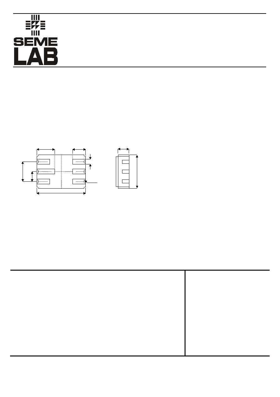
PIN OUT
Pin 1 ≠ Collector 1 Pin 4 ≠ Collector 2
Pin 2 ≠ Base 1
Pin 5 ≠ Emitter 2
Pin 3 ≠ Base 2 Pin 6 ≠ Emitter 1
DUAL BIPOLAR NPN DEVICES
IN A HERMETICALLY SEALED
LCC2 CERAMIC SURFACE MOUNT
PACKAGE FOR HIGH RELIABILITY
APPLICATIONS
FEATURES
∑ SILICON PLANAR EPITAXIAL NPN
TRANSISTOR
∑ HERMETIC CERAMIC SURFACE MOUNT
PACKAGE
∑ CECC SCREENING OPTIONS
∑ SPACE QUALITY LEVELS OPTIONS
∑ JAN LEVEL SCREENING OPTIONS
∑ HIGH VOLTAGE
All Semelab hermetically sealed products can
be processed in accordance with the
requirements of BS, CECC and JAN, JANTX,
JANTXV and JANS specifications.
LCC2 (MO-041BB)
MECHANICAL DATA
Dimensions in mm (inches)
2N3501DCSM
Semelab plc.
Telephone +44(0)1455 556565. Fax +44(0)1455 552612.
E-mail: sales@semelab.co.uk Website: http://www.semelab.co.uk
Document Number 4059
Issue 1
ABSOLUTE MAXIMUM RATINGS
(T
case
= 25∞C unless otherwise stated)
Single Side
Total Device
V
CBO
Collector-Base
Voltage
150V
V
CEO
Collector-Emitter Voltage(I
B
=0)
150V
V
EBO
Emitter-Base Voltage(I
B
=0)
6V
I
C
Continuous
Collector
Current
300mA
P
D
Power Dissipation Tamb = 25∞C
300mW
500mW
Derate above 25∞C
1.72mW/∞C
2.86mW/∞C
T
j
Operating Temperature Range
-65 to 200∞C
T
stg
Storage Temperature Range
-65 to 200∞C
R
thJA
Thermal Resistance Junction to Ambient
350∞C
1
2
6
3
4
5
2.54 ± 0.13
(0.10 ± 0.005)
0.64 ± 0.06
(0.025 ± 0.003)
0.23
(0.009)
1.40 ± 0.15
(0.055 ± 0.006)
1.65 ± 0.13
(0.065 ± 0.005)
2.29 ± 0.20
(0.09 ± 0.008)
rad.
A
1.27 ± 0.13
(0.05 ± 0.005)
A =
6.22 ± 0.13
(0.245 ± 0.005)
4.32 ± 0.13
(0.170 ± 0.005)
Semelab Plc reserves the right to change test conditions, parameter limits and package dimensions without notice. Information furnished by Semelab is believed
to be both accurate and reliable at the time of going to press. However Semelab assumes no responsibility for any errors or omissions discovered in its use.
Semelab encourages customers to verify that datasheets are current before placing orders.
2N3501DCSM
Semelab plc.
Telephone +44(0)1455 556565. Fax +44(0)1455 552612.
E-mail: sales@semelab.co.uk Website: http://www.semelab.co.uk
Document Number 4059
Issue 1
ELECTRICAL CHARACTERISTICS
(T
case
= 25
∞
C unless otherwise stated)
Parameter Test
Conditions
Min.
Typ.
Max.
Unit
OFF CHARACTERISTICS
V
(BR)CEO
Collector-Emitter Breakdown Voltage
1
I
C
=10mA
I
B
=0
150
V
V
(BR)CBO
Collector-Base Breakdown Voltage
I
C
=10µA I
E
=0
150
V
V
(BR)EBO
Emitter-Base Breakdown Voltage
I
E
=10µA I
C
=0
6
V
I
CBO
Collector Cutoff Current
V
CB
=75V I
E
=0
0.05
T
amb
=150
∞
C
50
µA
I
EBO
Emitter Cutoff Current
V
BE(off)
=4V V
CE
=0
25 nA
ON CHARACTERISTICS
I
C
=0.1mA V
CE
=10V
35
I
C
=1mA V
CE
=10V
50
I
C
=10 mA
V
CE
=10V
75
I
C
=150 mA
V
CE
=10V
100 300
h
FE
DC Current Gain
I
C
=300 mA
V
CE
=10V
20
I
C
=10mA
I
B
=1mA
0.2
I
C
=50mA
I
B
=5mA
0.25
V
CE(SAT)
Collector-Emitter Saturation Voltage
1
I
C
=150 mA
I
B
=15mA
0.4
V
I
C
=10mA
I
B
=1mA
0.8
I
C
=50mA
I
B
=5mA
0.9
V
BE(SAT)
Base-Emitter Saturation Voltage
1
I
C
=150 mA
I
B
=15mA
1.2
V
SMALL SIGNAL CHARACTERISTICS
f
T
Current Gain-Bandwidth Product
(100MHz)
V
CE
=20V I
C
=20mA
150
MHz
C
obo
Output Capacitance (1MHz)
V
CB
=10V I
E
=0
8
C
ibo
Input Capacitance (1MHz)
V
EB
=0.5V I
C
=0
80
pF
h
ie
Input Impedance (1kHz)
V
CE
=10V I
C
=10mA
0.25
1.25 `
h
fe
Small-Signal Current Gain (1kHz)
V
CE
=10V I
C
=10mA
375
h
oe
Output Admittance (1kHz)
V
CE
=10V I
C
=10mA
200 `
SWITCHING CHARACTERISTICS
t
d
Delay Time
I
C
=150mA I
B
1
=15mA
20
t
r
Rise Time
V
CC
=100V V
EB(off)
=-2V
35
t
s
Storage Time
I
C
=150mA I
B
1
=15mA
800
t
f
Fall Time
I
B1
=I
B2
=15mA
80
ns
1) Pulse Test: Pulse Width < 300µs, Duty Cycle <2%
2) ft is defined as frequency at which |hfe|.ftest
Semelab Plc reserves the right to change test conditions, parameter limits and package dimensions without notice. Information furnished by Semelab is believed
to be both accurate and reliable at the time of going to press. However Semelab assumes no responsibility for any errors or omissions discovered in its use.
Semelab encourages customers to verify that datasheets are current before placing orders.