Document Number 6051
Issue 1
Semelab plc.
Telephone +44(0)1455 556565. Fax +44(0)1455 552612.
E-mail:
sales@semelab.co.uk
Website:
http://www.semelab.co.uk
Semelab Plc reserves the right to change test conditions, parameter limits and package dimensions without notice. Information furnished by Semelab is believed
to be both accurate and reliable at the time of going to press. However Semelab assumes no responsibility for any errors or omissions discovered in its use.
Semelab encourages customers to verify that datasheets are current before placing orders.
2N3738
V
CBO
Collector ≠ Base Voltage
V
CEO
Collector ≠ Emitter Voltage (I
B
= 0)
V
EBO
Emitter ≠ Base Voltage (I
C
= 0)
I
C
Collector Current
I
C(PK)
Peak Collector Current
I
B
Base Current
P
D
Total Device Dissipation at T
case
= 25∞C
Derate 25∞C
T
stg
Operating and Storage Temperature Range
250V
225V
6V
1A
2A
0.5A
20W
0.133W/∞C
≠65 to 200∞C
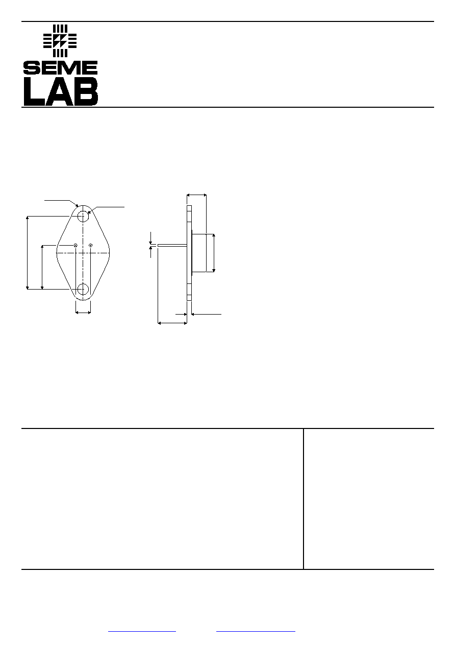
MECHANICAL DATA
Dimensions in mm
24.13 (0.95)
24.63 (0.97)
14.48 (0.570)
14.99 (0.590)
3.68
(0.145) rad.
max.
3.61 (0.142)
4.08(0.161)
rad.
0.71 (0.028)
0.86 (0.034)
1.27 (0.050)
1.91 (0.750)
9.14 (0.360)
min.
4.83 (0.190)
5.33 (0.210)
6.35 (0.250)
8.64 (0.340)
11.94 (0.470)
12.70 (0.500)
1
2
POWER TRANSISTORS
NPN SILICON
TO66 Package (TO-213AA)
ABSOLUTE MAXIMUM RATINGS
(T
case
= 25∞C unless otherwise stated)
FEATURES
∑ Hermetically Packaged.
∑ Low Saturation Voltage
∑ High Gain
Pin 1 = Base
Pin 2 = Emitter
Case = Collector

Document Number 6051
Issue 1
Semelab plc.
Telephone +44(0)1455 556565. Fax +44(0)1455 552612.
E-mail:
sales@semelab.co.uk
Website:
http://www.semelab.co.uk
Semelab Plc reserves the right to change test conditions, parameter limits and package dimensions without notice. Information furnished by Semelab is believed
to be both accurate and reliable at the time of going to press. However Semelab assumes no responsibility for any errors or omissions discovered in its use.
Semelab encourages customers to verify that datasheets are current before placing orders.
2N3738
Parameter
Test Conditions
Min.
Typ.
Max.
Unit
225
0.1
0.25
0.5
1.0
0.1
30
40
200
25
2.5
1.0
10
20
35
V
mA
mA
mA
mA
mA
--
V
MHz
pF
--
I
C
= 5mA
I
B
= 0
V
CB
= 250V
I
E
= 0
V
CE
= 125V
I
B
= 0
V
CE
= 250V
V
BE(OFF)
= 1.5V
V
CE
= 125V
V
BE(OFF)
= 1.5V
T
C
= 100∞C
V
EB
= 6V
I
C
= 50mA
V
CE
= 10V
I
C
= 100mA
V
CE
= 10V
I
C
= 250mA
V
CE
= 10V
I
C
= 250mA
I
B
= 25mA
I
C
= 100mA
V
CE
= 10V
I
C
= 100mA
V
CE
= 10V
f = 10MHz
V
CB
= 100V
I
E
= 0
f = 100KHz
I
C
= 100mA
V
CE
= 20V
f = 1KHz
ELECTRICAL CHARACTERISTICS
(Tcase = 25∞C unless otherwise stated)
Collector≠ Emitter Breakdown Voltage
Collector Base Cut≠Off Current
Collector Emiiter Cut≠Off Current
Collector Cut≠Off Current
Emitter Base Cut≠Off Current
DC Current Gain
Collector ≠ Emitter Saturation Voltage
Base ≠ Emitter on Voltage
Transition Frequency
Output Capacitance
Small Signal Current Gain
* Pulse Width
300
µ
s , Duty Cycle
<
2%
V
CEO(BR)*
I
CBO
I
CEO
I
CEV
I
EBO
h
FE*
V
CE(sat)*
V
BE(on)*
f
T
C
ob
h
fe
DYNAMIC CHARACTERISTICS
ELECTRICAL CHARACTERISTICS