V
CEO
Collector ≠ Emitter Voltage
V
CB
Collector ≠ Base Voltage
V
EB
Emitter ≠ Base Voltage
I
C
Collector Current
Continuous
I
C
Peak (1)
I
B
Base Current
P
D
Total Power Dissipation
Derate above 25 ∞C
T
J
, T
stg
Operating and Storage Junction Temperature Range
R
q
JC
Thermal Resistance , Junction To Case
300V
500V
6V
2A
5A
1A
35W
0.2W / ∞C
-65 to 200 ∞C
5.0∞C / W
LAB
SEME
2N4240
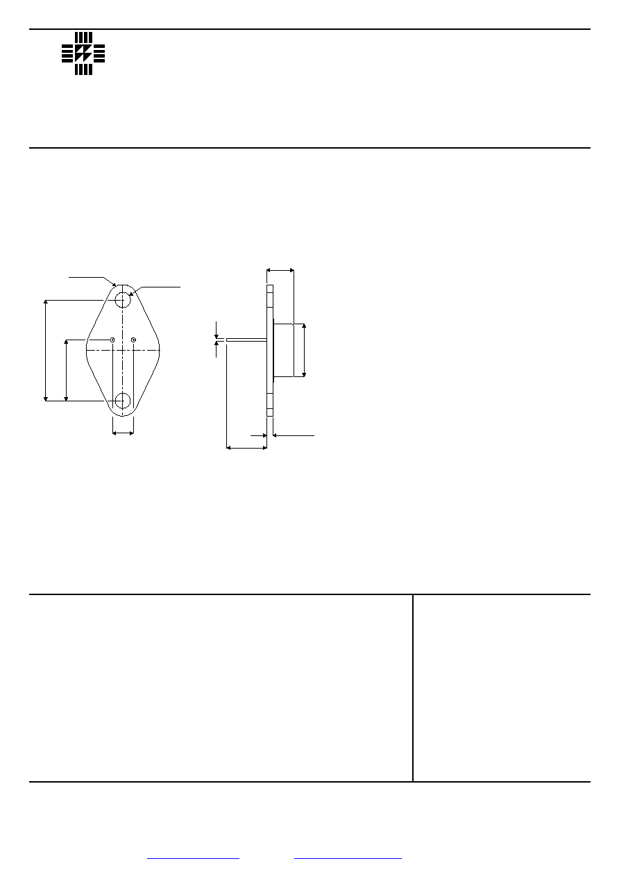
MECHANICAL DATA
Dimensions in mm
24.33 (0.958)
24.43 (0.962)
14.48 (0.570)
14.99 (0.590)
3.68
(0.145) rad.
max.
3.61 (0.142)
3.86 (0.145)
rad.
0.71 (0.028)
0.86 (0.034)
1.27 (0.050)
1.91 (0.750)
9.14 (0.360)
min.
4.83 (0.190)
5.33 (0.210)
6.35 (0.250)
8.64 (0.340)
11.94 (0.470)
12.70 (0.500)
NPN TRANSISTOR
MEDIUM POWER
HIGH VOLTAGE
APPLICATIONS
Designed for switching regulator
applications where high frequency and
high voltage swings are required.
TO66 Package.
ABSOLUTE MAXIMUM RATINGS
(T
case
=25∞C unless otherwise stated)
Prelim. 8/93
NOTES:
(1) Pulse Test: Pulse Width = 5.0 ms , Duty Cycle
£
10%.
Semelab plc.
Telephone +44(0)1455 556565. Fax +44(0)1455 552612.
E-mail:
sales@semelab.co.uk
Website:
http://www.semelab.co.uk

FIGURE 1 ≠ SWITCHING TIME TEST CIRCUIT
2N4240
Prelim. 8/93
ELECTRICAL CHARACTERISTICS
(Tcase = 25∞C , unless otherwise stated)
Collector ≠ Emitter
Sustaining Voltage
I
CEO
Collector Cutoff Current
I
CEX
Collector Cutoff Current
I
EBO
Emitter Cutoff Current
I
C
= 200mA , I
B
= 0
V
CE
= 150V , I
B
= 0
V
CE
= 450V , V
BE(off)
= 1.5V
V
CE
= 450V , V
BE(off)
= 1.5V , T
C
=150∞C
V
BE
= 6V , I
C
= 0
300
5.0
2.0
5.0
0.5
Parameter
Test Conditions
Min.
Typ.
Max.
Unit.
V
mA
mA
mA
Current Gain
Collector ≠ Emitter
Saturation Voltage
Base ≠ Emitter
Saturation Voltage
Base ≠ Emitter
On Voltage
Second Breakdown
Collector Current
I
C
= 0.1A , V
CE
= 10V
I
C
= 0.75A , V
CE
= 2V
I
C
= 0.75A , V
CE
= 10V
I
C
= 0.75A , I
B
= 75mA
I
C
= 0.75A , I
B
= 75mA
I
C
= 0.1A , V
CE
= 10V
(V
CC
= 100V)
40
10
100
30
150
1.0
1.8
1.4
350
Parameter
Test Conditions
Min.
Typ.
Max.
Unit.
--
V
V
V
mA
h
FE
V
CE(sat)
V
BE(sat)
V
BE(on)
I
s/b
Current Gain ≠
Bandwidth Product (2)
Output Capacitance
I
C
= 200mA , V
CE
= 10V
f
test
= 5.0MHz
V
CB
= 10V , I
E
= 0 , f = 1.0MHz
15
120
Parameter
Test Conditions
Min.
Typ.
Max.
Unit.
MHz
pF
f
T
C
ob
Rise Time
Storage Time
Fall Time
V
CC
= 200V , I
C
= 0.75A
R
L
= 200
W
, I
B1
= 100mA
V
CC
= 200V , I
C
= 0.75A
I
B1
= I
B2
= 75mA
V
CC
= 200V , I
C
= 0.75A
I
B1
= I
B2
= 75mA
0.5
6.0
3.0
Parameter
Test Conditions
Min.
Typ.
Max.
Unit.
m
S
m
S
m
S
t
r
t
s
t
f
OFF CHARACTERISTICS
ON CHARACTERISTICS
(1)
DYNAMIC CHARACTERISTICS
SWITCHING CHARACTERISTICS
NOTES:
(1) Pulse Test: Pulse Width = 300
m
s , Duty Cycle
£
2%
(2) f
T
=
|
h
fe
|
∑ f
test
RB AND RC varied to obtain desired current levels.
D1 must be fast recovery type.
For td and tr , D1 is disconnected and V2 = 0.
V
CEO(sus)
Semelab plc.
Telephone +44(0)1455 556565. Fax +44(0)1455 552612.
E-mail:
sales@semelab.co.uk
Website:
http://www.semelab.co.uk