BAT54DCSM
Document Number 3550
Issue 1
LAB
SEME
Semelab plc.
Telephone +44(0)1455 556565. Fax +44(0)1455 552612.
E-mail:
sales@semelab.co.uk
Website:
http://www.semelab.co.uk
Semelab Plc reserves the right to change test conditions, parameter limits and package dimensions without notice. Information furnished by Semelab is believed
to be both accurate and reliable at the time of going to press. However Semelab assumes no responsibility for any errors or omissions discovered in its use.
Semelab encourages customers to verify that datasheets are current before placing orders.
30V
200mA
600mA
200mW
2.0mW/∞C
≠55 to +125∞C
≠65 to +175∞C
V
R
Reverse Voltage
I
F
Forward Current (Each Diode)
I
FM
Peak Forward Current (Each Diode)
P
D
Power Dissipation (Each Diode)
Derate @ T
AMB
>25∞C
T
J
Maximum Operating Junction Temperature
T
STG
Storage Temperature Range
ABSOLUTE MAXIMUM RATINGS
(T
AMB
= 25∞C unless otherwise stated)
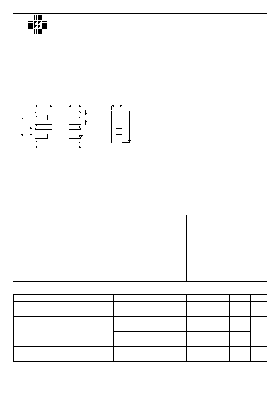
MECHANICAL DATA
Dimensions in mm (inches)
1
2
6
3
4
5
2.54 ± 0.13
(0.10 ± 0.005)
0.64 ± 0.06
(0.025 ± 0.003)
0.23
(0.009)
1.40 ± 0.15
(0.055 ± 0.006)
1.65 ± 0.13
(0.065 ± 0.005)
2.29 ± 0.20
(0.09 ± 0.008)
rad.
A
1.27 ± 0.13
(0.05 ± 0.005)
A =
6.22 ± 0.13
(0.245 ± 0.005)
4.32 ± 0.13
(0.170 ± 0.005)
DUAL SCHOTTKY DIODES IN
HERMETIC CERAMIC
SURFACE MOUNT PACKAGE
FOR HIGH RELIABILITY
APPLICATIONS
Parameter
Test Conditions
Min.
Typ.
Max.
Unit
I
R
Reverse Current
V
F
Forward Voltage
C
Capacitance
t
rr
Reverse Recovery Time
V
R
= 25V
V
R
= 25V
T
A
= 85∞C
I
F
= 1mA
I
F
= 10mA
I
F
= 30mA
V
R
= 1V
f = 1MHz
I
F
= 100mA to I
R
= 10mA
R
L
= 100
2
100
0.32
0.40
0.50
10
5
µ
A
V
pF
ns
ELECTRICAL CHARACTERISTICS
(T
AMB
= 25∞C unless otherwise stated)
LCC2 PACKAGE (MO-041BB)
PAD 1 -- Cathode 1 PAD 2 -- N/C
PAD 3 -- N/C
Underside View
PAD 4 -- Cathode 2 PAD 5 -- Anode 2 PAD 6 -- Anode 1